Switching VGA Signals in a Notebook
Introduction
Although digital video switching has become more popular in 2008, there are still tens of millions of monitors and projectors that dictate the use of analog VGA support until at least 2015. Nearly all enterprise notebook computers, which employ a docking station, switch VGA signals through a set of connectors at the base of the notebook.An ideal device to handle the switching between the dock and the VGA connector manages all the switching and has adequate ESD protection for all outputs connected to a port connector.
The MAX4885E VGA switch is optimized for signal switching between a notebook and docking station. The device contains three very high-frequency (~950MHz) switches for RGB, two low-frequency clamping switches for the DDC signals, and a pair of level-translating buffers for the horizontal and vertical signals.
Optimized VGA Switching
To handle the analog VGA signal properly, the seven signals should be routed either to the rear connector on the computer or to the docking port. If this function is not switched, either port could be connected while not in use, thus adding considerable capacitance to the DAC and causing bandwidth to roll off. Video signals are usually standardized to 75Ω impedance, and the video DAC is normally a current source driving a 75Ω load. The monitor is a 75Ω load as well, providing for a doubly terminated system. Maximum output of the DAC into a 75Ω load is 0.7V for VGA.Many designers try to achieve 1920 x 1200, 60Hz, which yields a pixel rate of ≈6.0ns. If we permit a rise and fall time of 1.7ns (each), the signal will pass the VESA (Video Electronics Standards Association) requirements. Therefore:
tR = 2.2RC, where R= 37.5Ω
This equation would yield the tR for the system, if the DAC had a tR of 0. A typical DAC for this application may, however, have a tR of 1ns, without any further loading. The DAC is assumed to have two components of delay, internal delay and rise time, owing to its output capacitance. For this discussion, the DAC will be assumed to have 300ps internal delay and 8pf capacitance. This permits the total capacitance to be ≈16pF, with a total of 8pF allowed for the switch. Many of the older analog switches used for this function were rated at 400MHz, f3dB bandwidth. Although this would seem adequate for a 140Msps signal, the DAC uses much of the system's margin.
MAX4885E VGA Switch Reduces Component Count
The MAX4885E is a complete VGA 1:2 switch with > 700MHz of bandwidth and < 7pF capacitance for the RGB switching. In addition, these outputs are protected to the level of ±15kV HBM (Human Body Model), so no added ESD protection will be needed. Not only does this design save cost, but it eliminates the need for extra capacitance caused by the protection devices.The MAX4885E has two additional important functions; it translates the low-level horizontal and vertical signals to 5.0V-compatible TTL
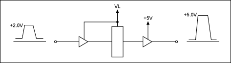
Figure 1. Schematic for a horizontal and vertical translator.
signals, in accordance with the VESA specification (Figure 1). One set of horizontal and vertical outputs is provided to drive both loads. As with the RGB signals, the horizontal and vertical signals are protected to ±15kV so no added components should be necessary to protect their output. By tying the VL pin to +3.3V, the horizontal and vertical signals are translated from low level to full TTL compatibility.
The MAX4885E also provides DDC (display data control) switching, level clamping, and ESD protection. By switching the DDC signals, the capacitive load is split. These signals are I²C compatible and subject to a maximum loading of 700pF. If two loads are placed on the same output the capacitive loading can be exceeded. The MAX4885E only permits one load to be present at a time. Like the other functions, the DDC outputs are protected to ±15kV ESD. There is one final function that the MAX4885E DDC switch provides for the application: voltage clamping. The DDC voltage from a monitor is normally pulled up to +5V through a 2.2kΩ resistor (Figure 2). This voltage is not permitted to appear on the DDC driver device, which normally allows a +3.3V maximum. The DDC signals are I²C compatible, with pull-up resistors on each side of the switch. The switch itself is comprised of a pair of n-channel transistors.
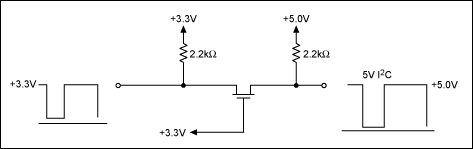
Figure 2. Schematic for an n-channel FET translator clamp.
Because of the body-effect, an n-channel FET can only pass signals to within ~0.7V of the gate voltage. As the voltage approaches the gate voltage, the channel resistance increases because of a lack of bias. Since both sides of the switch are pulled up to their respective supplies, the n-channels is a nearly perfect clamp. There is no problem passing a signal near ground, so the switch facilitates the pulldown. If the +5V side swings from 0.5V to 4.8V, then the 3.3V side will swing from 0.5V to 3.3V, as seen above (left).