摘要:本文旨在帮助工程师快速掌握MAX6954驱动7段单色LED驱动器的使用方法。
MAX6954是一个通用显示驱动器,能够通过一个串口控制多个分立、7段、14段或16段LED显示器。本篇应用笔记介绍驱动8位单色、7段LED显示器的典型应用与配置。
有关MAX6954的详细信息请参考MAX6954的数据资料。
应用笔记"快速入门:使用MAX6954驱动16段LED显示器" 和"快速入门:使用MAX6954驱动14段LED显示器" 与本文类似,分别介绍了如何配置MAX6954驱动16段和14段显示器。
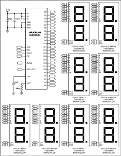
放大显示
图1. MAX6954驱动7段显示器电路
MAX6954的一个常见应用是驱动多达16位的7段单色LED。本篇应用笔记指导用户如何连接MAX6954与7段显示器,以及如何配置其内部寄存器控制显示十六进制字符。
MAX6954使用一种交替改变驱动器端口极性的复用技术来减少引脚数目。这与驱动器阴极和阳极引脚单独使用的标准LED复用连接方式不同。应用笔记 "Charlieplexing - Reduced Pin-Count LED Display MulTIplexing" 对这一技术进行了讨论。表1为MAX6954与7段显示器的连线表,此表兼容于MAX6954的复用配置及其十六进制字符的内置字模。表1中的字母对应于图2中的段标识。图1为MAX6954驱动十六位7段显示器的电路示意图。
表1.与16位7段显示器连线表
| Digit |
O0 |
O1 |
O2 |
O3 |
O4 |
O5 |
O6 |
O7 |
O8 |
O9 |
O10 |
O11 |
O12 |
O13 |
O14 |
O15 |
O16 |
O17 |
O18 |
0,
0a |
CC0 |
-- |
1a |
-- |
1b |
1c |
1d |
1dp |
1e |
1f |
1g |
2a |
2b |
2c |
2d |
2e |
2f |
2g |
2dp |
1,
1a |
-- |
CC1 |
1a |
-- |
1b |
1c |
1d |
1dp |
1e |
1f |
1g |
2a |
2b |
2c |
2d |
2e |
2f |
2g |
2dp |
2,
2a |
1a |
-- |
CC2 |
-- |
1b |
1c |
1d |
1dp |
1e |
1f |
1g |
2a |
2b |
2c |
2d |
2e |
2f |
2g |
2dp |
3,
3a |
1a |
-- |
-- |
CC3 |
1b |
1c |
1d |
1dp |
1e |
1f |
1g |
2a |
2b |
2c |
2d |
2e |
2f |
2g |
2dp |
4,
4a |
1a |
-- |
1b |
1c |
CC4 |
-- |
1d |
1dp |
1e |
1f |
1g |
2a |
2b |
2c |
2d |
2e |
2f |
2g |
2dp |
5,
5a |
1a |
-- |
1b |
1c |
-- |
CC5 |
1d |
1dp |
1e |
1f |
1g |
2a |
2b |
2c |
2d |
2e |
2f |
2g |
2dp |
6,
6a |
1a |
-- |
1b |
1c |
1d |
1dp |
CC6 |
-- |
1e |
1f |
1g |
2a |
2b |
2c |
2d |
2e |
2f |
2g |
2dp |
7,
7a |
1a |
-- |
1b |
1c |
1d |
1dp |
-- |
CC7 |
1e |
1f |
1g |
2a |
2b |
2c |
2d |
2e |
2f |
2g |
2dp |
完成MAX6954与7段显示器连线后,可利用显示测试模式检查连线正确性。显示测试模式不受控制和数据寄存器影响,点亮显示器所有的段,但不改变任何寄存器内容。向寄存器0x07写入0x01启动显示测试模式。测试模式下显示器如果有不亮的段则说明连线有误。向寄存器0x07写入0x00退出显示测试模式。
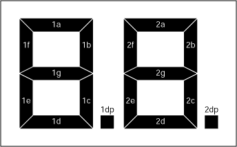
图2. 7段显示器的段标识
完成连线检查后,需要按驱动7段显示器的要求设置MAX6954寄存器值。表2包括MAX6954一些重要寄存器的上电初始值。MAX6954初次上电时处于关断模式,各位显示消隐,选择7段字模并将扫描位数设为最大,即八位。通过向寄存器0x0C写入0xFF可将MAX6954设置成驱动7段显示器的模式。译码模式寄存器(0x01)的默认值适用于7段显示器。
表2.MAX6954寄存器上电初始状态
| REGISTER |
POWER-UP CONDITION |
ADDRESS
(HEX) |
REGISTER DATA |
| D7 |
D6 |
D5 |
D4 |
D3 |
D2 |
D1 |
D0 |
| Decode Mode |
7-segment font enabled |
0x01 |
1 |
1 |
1 |
1 |
1 |
1 |
1 |
1 |
| Global Intensity |
1/16 (minimum intensity) |
0x02 |
X |
X |
X |
X |
0 |
0 |
0 |
0 |
| Scan Limit |
Display sixteen 7-segment digits: 0, 1, 2, 3, 4, 5, 6, 7, 0a, 1a, 2a, 3a, 4a, 5a, 6a, 7a |
0x03 |
X |
X |
X |
X |
X |
1 |
1 |
1 |
| Control Register |
Shutdown enabled, blink disabled, blink speed is slow |
0x04 |
0 |
0 |
X |
X |
0 |
0 |
0 |
0 |
| Display Test |
Normal operaTIon (display test disabled) |
0x07 |
X |
X |
X |
X |
X |
X |
X |
0 |
| Digit Type |
Digits 0 through 7 are 7 segment digits |
0x0C |
0 |
0 |
0 |
0 |
0 |
0 |
0 |
0 |
| Intensity10 |
1/16 (min on), digits 1 and 0 |
0x10 |
0 |
0 |
0 |
0 |
0 |
0 |
0 |
0 |
| Intensity32 |
1/16 (min on), digits 3 and 2 |
0x11 |
0 |
0 |
0 |
0 |
0 |
0 |
0 |
0 |
| Intensity54 |
1/16 (min on), digits 5 and 4 |
0x12 |
0 |
0 |
0 |
0 |
0 |
0 |
0 |
0 |
| Intensity76 |
1/16 (min on), digits 7 and 6 |
0x13 |
0 |
0 |
0 |
0 |
0 |
0 |
0 |
0 |
| Intensity10a |
1/16 (min on), digits 1a and 0a |
0x14 |
0 |
0 |
0 |
0 |
0 |
0 |
0 |
0 |
| Intensity32a |
1/16 (min on), digits 3a and 2a |
0x15 |
0 |
0 |
0 |
0 |
0 |
0 |
0 |
0 |
| Intensity54a |
1/16 (min on), digits 5a and 4a |
0x16 |
0 |
0 |
0 |
0 |
0 |
0 |
0 |
0 |
| Intensity76a |
1/16 (min on), digits 7a and 6a |
0x17 |
0 |
0 |
0 |
0 |
0 |
0 |
0 |
0 |
| Digit 0 |
Blank digit, both planes |
0x60 |
0 |
0 |
1 |
0 |
0 |
0 |
0 |
0 |
| Digit 1 |
Blank digit, both planes |
0x61 |
0 |
0 |
1 |
0 |
0 |
0 |
0 |
0 |
| Digit 2 |
Blank digit, both planes |
0x62 |
0 |
0 |
1 |
0 |
0 |
0 |
0 |
0 |
| Digit 3 |
Blank digit, both planes |
0x63 |
0 |
0 |
1 |
0 |
0 |
0 |
0 |
0 |
| Digit 4 |
Blank digit, both planes |
0x64 |
0 |
0 |
1 |
0 |
0 |
0 |
0 |
0 |
| Digit 5 |
Blank digit, both planes |
0x65 |
0 |
0 |
1 |
0 |
0 |
0 |
0 |
0 |
| Digit 6 |
Blank digit, both planes |
0x66 |
0 |
0 |
1 |
0 |
0 |
0 |
0 |
0 |
| Digit 7 |
Blank digit, both planes |
0x67 |
0 |
0 |
1 |
0 |
0 |
0 |
0 |
0 |
| Digit 0a |
Blank digit, both planes |
0x68 |
0 |
0 |
1 |
0 |
0 |
0 |
0 |
0 |
| Digit 1a |
Blank digit, both planes |
0x69 |
0 |
0 |
1 |
0 |
0 |
0 |
0 |
0 |
| Digit 2a |
Blank digit, both planes |
0x6A |
0 |
0 |
1 |
0 |
0 |
0 |
0 |
0 |
| Digit 3a |
Blank digit, both planes |
0x6B |
0 |
0 |
1 |
0 |
0 |
0 |
0 |
0 |
| Digit 4a |
Blank digit, both planes |
0x6C |
0 |
0 |
1 |
0 |
0 |
0 |
0 |
0 |
| Digit 5a |
Blank digit, both planes |
0x6D |
0 |
0 |
1 |
0 |
0 |
0 |
0 |
0 |
| Digit 6a |
Blank digit, both planes |
0x6E |
0 |
0 |
1 |
0 |
0 |
0 |
0 |
0 |
| Digit 7a |
Blank digit, both planes |
0x6F |
0 |
0 |
1 |
0 |
0 |
0 |
0 |
0 |
配置寄存器(0x04)用来设置进入和退出关断模式,控制闪烁功能,全局清除各位数据,以及选择对各位亮度进行全局还是单独控制。配置寄存器包含7位(见表3)。
- S 位用来选择关断模式还是正常工作模式(读/写)。
- B 位用来选择闪烁速率(读/写)。
- E 位用来全局启动或禁止闪烁功能(读/写)。
- T 位用来复位闪烁时序(此数据不被存储―瞬态位)。
- R 位用来全局清除所有显示位对应的P0和P1两级寄存器(此数据不被存储―瞬态位)。
- I 位用来选择对各位亮度进行全局还是单独控制(读/写)。
- P 位用来返回当前闪烁时序相位(只读―向此位写入值将被忽略)。
表3. 配置寄存器格式
CONFIGURATION
REGISTER
DATA BIT |
DATA BIT LABEL |
STATE |
FUNCTION |
| D7 |
P |
0 |
P1 Blink Phase |
| D6 |
I |
0 |
Intensity for all digits is controlled by one setting in the Global Intensity Register |
| 1 |
Intensity for digits is controlled by the individual settings in the Intensity10 through Intensity76a registers. |
| D5 |
R |
0 |
Digit data for both planes P0 and P1 are unaffected |
| 1 |
Digit data for both planes P0 and P1 are cleared on the rising edge of active-low CS |
| D4 |
T |
0 |
Blink timing counters are unaffected. |
| 1 |
Blink timing counters are reset on the rising edge of active-low CS. |
| D3 |
E |
0 |
Blink function disabled |
| 1 |
Blink function enabled |
| D2 |
B |
0 |
Slow Blinking. Segments blink on for 1s, off for 1s with fOSC = 4MHz. |
| 1 |
Fast Blinking. Segments blink on for 0.5s, off for 0.5s with fOSC = 4MHz. |
| D1 |
X |
X |
Don't care |
| D0 |
S |
0 |
Shutdown |
| 1 |
Normal Operation |
通过向寄存器0x04写入0x01启动显示器驱动器,同时将工作方式设置为全局亮度控制、禁止闪烁。内部振荡器在MAX6954退出关断模式时启动,振荡器输出引脚为OSC_OUT。注意,数据控制寄存器0x60至0x67上电状态为0x20或没有段被点亮时,7段显示器保持显示消隐(见表2和图3)。
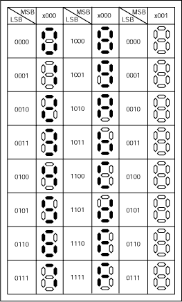
图3. 7段显示器字模
MAX6954内置了用于7段显示器的十六进制字模,用7位表示十六进制字符,第8位用于选择是否点亮小数点(DP)(见表4)。数据寄存器有两级,P0和P1。每个显示位用存储器中的2字节表示,一个字节位于P0,另一个位于P1(见表7)。数据寄存器为映射地址方式,所以每位数据可在P0(寄存器0x20至0x2F)中更新,也可在P1(寄存器0x20至0x4 F)中更新,还可以两级同时更新(寄存器0x60至0x67)。数据寄存器中的数据并不直接控制7段显示器中各段的显示。而是被用来寻址存储7段字模数据的字符发生器(见图3)。寄存器数据低7位(D6至D0)用来从字模中选择字符。最高位(D7)控制小数点(DP)显示;置为1则显示DP,置为0则不显示DP。
表4. 数字类型数据寄存器格式
| MODE |
ADDRESS CODE (HEX) |
REGISTER DATA |
| D7 |
D6 |
D5 |
D4 |
D3 |
D2 |
D1 |
D0 |
| 7-segment mode, writing digit data to use font map data with decimal place unlit |
0x20 to 0x2F
0x40 to 0x4F
0x60 to 0x6F |
0 |
Bits D6 to D0 select font character |
| 7-segment mode, writing digit data to use font map data with decimal place lit |
0x20 to 0x2F
0x40 to 0x4F
0x60 to 0x6F
| 1 |
Bits D6 to D0 select font character |
如果闪烁功能被配置寄存器闪烁使能位E(见表3)禁止,则P0中数据寄存器的数据被用作显示器复用。而P1中数据寄存器的数据不被使用。如果闪烁功能被启用,则交替使用P0和P1中的数据复用显示器。P0和P1中的数据分别应用于闪烁时钟交替变化的不同相位,从而复用LED显示器实现闪烁功能。
下面是一个利用MAX6954驱动显示Maxim/Dallas销售部电话:1 800 629 4642的实例。设置配置寄存器禁止闪烁功能,这样就可以通过向寄存器0x20至0x2F写入数据来分别控制数据位0至7。使用图3中的字模图得到每个字符对应的代码。
表 5. 电话 800.629.4642 范例
| REGISTER ADDRESS (HEX) |
DIGIT |
CHARACTER |
FONT MAP EQUIVALENT CODE |
| DECIMAL |
HEX |
| 0x20 |
0 |
C |
0000 1100 |
0x0C |
| 0x28 |
0a |
A |
0000 1001 |
0x0A |
| 0x21 |
1 |
1 |
0000 0001 |
0x01 |
| 0x29 |
1a |
1 |
0000 0001 |
0x01 |
| 0x23 |
3 |
8 |
0000 1000 |
0x08 |
| 0x2B |
3a |
0 |
0000 0000 |
0x00 |
| 0x24 |
4 |
0 |
1000 0000 |
0x80 |
| 0x2C |
4a |
6 |
0000 0110 |
0x06 |
| 0x25 |
5 |
2 |
0000 0010 |
0x02 |
| 0x2D |
5a |
9 |
1000 1001 |
0x89 |
| 0x26 |
6 |
4 |
0000 0100 |
0x04 |
| 0x2E |
6a |
6 |
0000 0110 |
0x06 |
| 0x27 |
7 |
4 |
0000 0100 |
0x04 |
| 0x2F |
7a |
2 |
0000 0010 |
0x02 |
通过向寄存器0x02(全局亮度控制寄存器)写入数据来调节显示亮度,亮度可在0x00(最小亮度,1/16的电流)和0xFF(最大亮度,15/16的电流)之间调节。也可以对每一位的亮度进行单独控制。关于显示亮度调节和其它先进特性(如GPIO和按键扫描)的详细信息请参考MAX6954的数据资料。
表 6. 例程命令集
REGISTER
(HEX) |
COMMAND
(HEX) |
FUNCTION |
| 0x07 |
0x01 |
Enter display test mode |
| 0x07 |
0x00 |
Exit display test mode |
| 0x04 |
0x01 |
Exit shutdown mode, disable blinking and select global intensity control |
| 0x20 |
0x0C |
Write "C" to digit 0 |
| 0x28 |
0x0A |
Write "A" to digit 0a |
| 0x21 |
0x01 |
Write "1" to digit 1 |
| 0x29 |
0x01 |
Write "1" to digit 1a |
| 0x23 |
0x08 |
Write "8" to digit 3 |
| 0x2B |
0x00 |
Write "0" to digit 3a |
| 0x24 |
0x80 |
Write "0." to digit 4 |
| 0x2C |
0x06 |
Write "6" to digit 4a |
| 0x25 |
0x02 |
Write "2" to digit 5 |
| 0x2D |
0x89 |
Write "9." to digit 5a |
| 0x26 |
0x04 |
Write "4" to digit 6 |
| 0x2E |
0x06 |
Write "6" to digit 6a |
| 0x27 |
0x04 |
Write "4" to digit 7 |
| 0x2F |
0x02 |
Write "2" to digit 7a |
| 0x02 |
0xFF |
Set global intensity to full-scale |
表 7. MAX6954/MAX6955的部分寄存器地址图
| REGISTER |
ADDRESS (COMMAND BYTE) |
ADDRESS
(HEX CODE) |
| D15 |
D14 |
D13 |
D12 |
D11 |
D10 |
D9 |
D8 |
| Decode Mode |
R/active-low W |
0 |
0 |
0 |
0 |
0 |
0 |
1 |
0x01 |
| Global Intensity |
R/active-low W |
0 |
0 |
0 |
0 |
0 |
1 |
0 |
0x02 |
| Scan Limit |
R/active-low W |
0 |
0 |
0 |
0 |
0 |
1 |
1 |
0x03 |
| Configuration |
R/active-low W |
0 |
0 |
0 |
0 |
1 |
0 |
0 |
0x04 |
| Display Test |
R/active-low W |
0 |
0 |
0 |
0 |
1 |
1 |
1 |
0x07 |
| Digit Type |
R/active-low W |
0 |
0 |
0 |
1 |
1 |
0 |
0 |
0x0C |
| Intensity 10 |
R/active-low W |
0 |
0 |
1 |
0 |
0 |
0 |
0 |
0x10 |
| Intensity 32 |
R/active-low W |
0 |
0 |
1 |
0 |
0 |
0 |
1 |
0x11 |
| Intensity 54 |
R/active-low W |
0 |
0 |
1 |
0 |
0 |
1 |
0 |
0x12 |
| Intensity 76 |
R/active-low W |
0 |
0 |
1 |
0 |
0 |
1 |
1 |
0x13 |
| Intensity 10a |
R/active-low W |
0 |
0 |
1 |
0 |
1 |
0 |
0 |
0x14 |
| Intensity 32a |
R/active-low W |
0 |
0 |
1 |
0 |
1 |
0 |
1 |
0x15 |
| Intensity 54a |
R/active-low W |
0 |
0 |
1 |
0 |
1 |
1 |
0 |
0x16 |
| Intensity 76a |
R/active-low W |
0 |
0 |
1 |
0 |
1 |
1 |
1 |
0x17 |
| Digit 0 Plane P0 |
R/active-low W |
0 |
1 |
0 |
0 |
0 |
0 |
0 |
0x20 |
| Digit 1 Plane P0 |
R/active-low W |
0 |
1 |
0 |
0 |
0 |
0 |
1 |
0x21 |
| Digit 2 Plane P0 |
R/active-low W |
0 |
1 |
0 |
0 |
0 |
1 |
0 |
0x22 |
| Digit 3 Plane P0 |
R/active-low W |
0 |
1 |
0 |
0 |
0 |
1 |
1 |
0x23 |
| Digit 4 Plane P0 |
R/active-low W |
0 |
1 |
0 |
0 |
1 |
0 |
0 |
0x24 |
| Digit 5 Plane P0 |
R/active-low W |
0 |
1 |
0 |
0 |
1 |
0 |
1 |
0x25 |
| Digit 6 Plane P0 |
R/active-low W |
0 |
1 |
0 |
0 |
1 |
1 |
0 |
0x26 |
| Digit 7 Plane P0 |
R/active-low W |
0 |
1 |
0 |
0 |
1 |
1 |
1 |
0x27 |
| Digit 0a Plane P0 |
R/active-low W |
0 |
1 |
0 |
1 |
0 |
0 |
0 |
0x28 |
| Digit 1a Plane P0 |
R/active-low W |
0 |
1 |
0 |
1 |
0 |
0 |
1 |
0x29 |
| Digit 2a Plane P0 |
R/active-low W |
0 |
1 |
0 |
1 |
0 |
1 |
0 |
0x2A |
| Digit 3a Plane P0 |
R/active-low W |
0 |
1 |
0 |
1 |
0 |
1 |
1 |
0x2B |
| Digit 4a Plane P0 |
R/active-low W |
0 |
1 |
0 |
1 |
1 |
0 |
0 |
0x2C |
| Digit 5a Plane P0 |
R/active-low W |
0 |
1 |
0 |
1 |
1 |
0 |
1 |
0x2D |
| Digit 6a Plane P0 |
R/active-low W |
0 |
1 |
0 |
1 |
1 |
1 |
0 |
0x2E |
| Digit 7a Plane P0 |
R/active-low W |
0 |
1 |
0 |
1 |
1 |
1 |
1 |
0x2F |
| Digit 0 Plane P1 |
R/active-low W |
1 |
0 |
0 |
0 |
0 |
0 |
0 |
0x40 |
| Digit 1 Plane P1 |
R/active-low W |
1 |
0 |
0 |
0 |
0 |
0 |
1 |
0x41 |
| Digit 2 Plane P1 |
R/active-low W |
1 |
0 |
0 |
0 |
0 |
1 |
0 |
0x42 |
| Digit 3 Plane P1 |
R/active-low W |
1 |
0 |
0 |
0 |
0 |
1 |
1 |
0x43 |
| Digit 4 Plane P1 |
R/active-low W |
1 |
0 |
0 |
0 |
1 |
0 |
0 |
0x44 |
| Digit 5 Plane P1 |
R/active-low W |
1 |
0 |
0 |
0 |
1 |
0 |
1 |
0x45 |
| Digit 6 Plane P1 |
R/active-low W |
1 |
0 |
0 |
0 |
1 |
1 |
0 |
0x46 |
| Digit 7 Plane P1 |
R/active-low W |
1 |
0 |
0 |
0 |
1 |
1 |
1 |
0x47 |
| Digit 0a Plane P1 |
R/active-low W |
1 |
0 |
0 |
1 |
0 |
0 |
0 |
0x48 |
| Digit 1a Plane P1 |
R/active-low W |
1 |
0 |
0 |
1 |
0 |
0 |
1 |
0x49 |
| Digit 2a Plane P1 |
R/active-low W |
1 |
0 |
0 |
1 |
0 |
1 |
0 |
0x4A |
| Digit 3a Plane P1 |
R/active-low W |
1 |
0 |
0 |
1 |
0 |
1 |
1 |
0x4B |
| Digit 4a Plane P1 |
R/active-low W |
1 |
0 |
0 |
1 |
1 |
0 |
0 |
0x4C |
| Digit 5a Plane P1 |
R/active-low W |
1 |
0 |
0 |
1 |
1 |
0 |
1 |
04D |
| Digit 6a Plane P1 |
R/active-low W |
1 |
0 |
0 |
1 |
1 |
1 |
0 |
0x4E |
| Digit 7a Plane P1 |
R/active-low W |
1 |
0 |
0 |
1 |
1 |
1 |
1 |
0x4F |