IntroducTIon
The DS1050 is a 5-bit programmable Pulse Width Modulator (PWM) that allows you to vary the duty cycle "on-the-fly" from 0 to 100% in 3.125% increments. It is controlled by a 2-wire serial interface that can address up to eight DS1050s on a single 2-wire bus. It is available in both an 8-pin SOIC and an 8-pin µSOP package in the following frequencies: 1kHz, 5kHz, 10kHz, and 25kHz. A DS1052 is also available, which is a 100kHz version of the DS1050.This applicaTIon note shows examples using a DS1050 as a DC fan controller and as a backlight brightness controller for an LED backlit LCD. In addiTIon, this application note will show how to interface multiple DS1050s on a single 2-wire bus. Firmware for an 8051 based system is included in Appendix A.
System Overview
The reference schematic in Figure 1 is divided into two subsystems, the DC fan motor controller block and the LCD LED backlight controller block. In addition, it shows a microcontroller as the 2-wire master and how it interfaces to the 2-wire slaves, the DS1050s.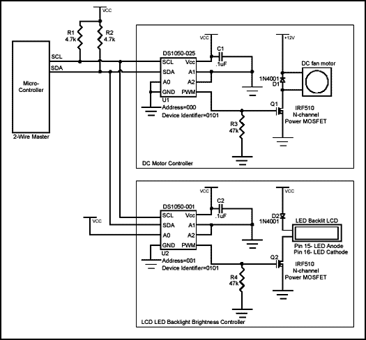
Figure 1. Reference schematic.
2-Wire Interface
The 2-wire master is implemented using open-drain outputs (one of which must be input and output) along with pull-up resistors R1 and R2 to generate the SDA (serial data) and SCL (serial clock) signals. The values given for R1 and R2 in the reference schematic will work fine for most applications, but these may need to be recalculated depending on the bus capacitance and the desired communication speed. Additional 2-wire devices can be added to the bus by connecting its SDA and SCL to the master's SDA and SCL pins. Address pins A0, A1, and A2 need to be tied high or low in order to give each device on the bus a unique address. The DS1050 (U1) in the schematic has all three address pins tied to ground, giving it a slave address of '000'. The DS1050 (U2) is set to a slave address of '001', however, any address other than U1's address will work. These address pins, along with the DS1050 "family code", or device identifier of '0101' are then used by the master to communicate with each slave individually.Figure 2 shows how these bits are used in a typical 2-wire transaction. After the 2-wire master generates a START condition, the Control Byte is sent (MSBit first) to select a particular device on the 2-wire bus. All devices on the bus "listen" to the Control Byte and check to see if it matches its own device identifier and slave address. The device that matches will respond by pulling SDA low to ACK. The LSBit of the Control Byte contains the R/W bit. This bit determines who will transmit the next byte, the Data Byte. If the R/W bit is set to a '1', then the master will read from the slave. So the master would then clock in the Data Byte from the slave. If the R/W bit was a '0', then the master will transmit the Data Byte to the slave. The 3 MSBits of the Data Byte can be thought of as opcodes, or instructions. For example, if these were '110', the master is instructing the DS1050 to enter shutdown mode. If these 3 bits are '000', then the next 5-bits, the PWM data, will set a new PWM duty cycle to output. After the Data Byte is transmitted (or received), an ACK (following a write) or a NACK (following a read) must be performed. An ACK (from slave) indicates that that it received the data during the write. A NACK (generated by the master) informs the slave that the master received the byte and does not want any more data. If the DS1050 had more registers, the master can also ACK (instead of NACK), indicating that he [the master] received the byte and wants to continue reading. Communication ends when the master issues a STOP condition.
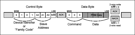
Figure 2. Typical 2-Wire transaction.
Figure 3 shows several examples of specific 2-wire instructions. A complete list of instructions can be found in the DS1050 datasheet
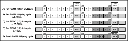
Figure 3. Example 2-Wire transactions.
While only eight DS1050s can be on a single 2-wire bus, other 2-wire devices can be added to the bus as long as its device identifier is not identical to the DS1050's. This is very useful to control additional 2-wire devices such as temperature sensors or digital pots.
For example 8051 based firmware showing how to communicate and control both DS1050s, look in Appendix A. Also, for additional information regarding the 2-wire interface, refer to the DS1050 datasheet.
DC Fan Motor Controller
The DC motor controller block of the reference schematic in Figure 1 shows a simple way to control a 12V DC fan motor using U1, a DS1050-025, to generate a 25kHz pulse-width-modulated signal which controls the average power delivered to the motor. A low duty cycle produces low average power, and in turn, a lower speed. As the duty cycle is increased, so does the amount of "on" time. The average power and speed increase. A duty cycle of 0% means that the motor is completely off, while a duty cycle of 50% means that the motor is on at half power. Also, when working with motors, it is important to be aware of the extra energy required to start the motor. In other words, don't set the duty cycle to 3.125% and expect the motor to turn. The motor you use will have a spec associated with this phenomenon. Likewise, when a motor has a large load and is expected to make a large jump in speed, the motor may stall if it is not incremented in several smaller steps. These are not work-arounds, but are instead a result of the laws of physics. Fortunately, these are easy to implement in firmware once you know they exist (although the included firmware is open loop and does not implement either of these cases).Choosing a PWM frequency
When interfacing a PWM to a motor, it is important that the PWM frequency not be within the audio spectrum. Otherwise, the motor will act like a speaker and produce an audible tone of the PWM frequency. Hence, the 25kHz version was used in the reference schematic.
Additional considerations that need to be made when choosing a PWM frequency are power consumption, EMI radiation, and output stage limitations. Theoretically, the difference in current consumption between the 25kHz and the 100kHz version is 4x as indicated by I=CVf, with all other things constant. Ironically, the 100kHz version only consumes 300µA of current, but the motor pulls orders of magnitudes more.
Although EMI radiation is not always an initial design consideration, if system EMI radiation is later a problem (due to other components), you may investigate which version of the DS1050 will contribute the least to the problem frequency.
Finally, if for some reason you are required to use a particular power MOSFET for Q1, you will need to check the MOSFET's gate threshold voltage to see if it can be driven directly from the 5V digital PWM without the need of any level translations. Also, you will need to verify that the MOSFET can handle the PWM frequency you are considering.
Driver Circuit
The digital PWM output of the DS1050 swings from ground to Vcc at the rated frequency and programmed duty cycle. The power-up default duty cycle is 50%. The PWM output controls the gate of Q1, an n-channel power MOSFET, which is capable of handling the current required by the 12V motor. Typical motor currents can be anywhere from 100mA to 500mA. The gate threshold voltage of Q1 is 2.0-4.0V. The DS1050 will have no problem directly driving the gate of Q1.
The 1N40018 diode, D1, is required across the supply terminals of the motor to clamp any back-EMF generated when the fan is off but still spinning due to its momentum. This is especially important when using pulse-width-modulation since while the fan is in normal operation, its power is being cycled 25,000 times a second. During the "off" times, the fan is spinning and the motor then becomes a generator and generates back-EMF.
When the DS1050 is instructed to enter shutdown mode, the PWM output floats. Therefore, to keep the gate of Q1 in a known state during shutdown, a pull-down resistor, R3, is used to make sure the fan is off. This resistor can also be used as a pull-up if you want the motor to turn on when the DS1050 is in shutdown, although this does defeat the purpose of going into shutdown.
Like always, it is important that sufficient decoupling be provided. Likewise, it is important that the decoupling capacitor, C1, has good high frequency performance and physically located as close as possible to U1 using short PCB traces.
Additional Notes
Although PWM is great for controlling standard DC motors, additional research will be needed if you plan to use the tachometer output found on some DC motors. Since the tachometer output of these fans are usually open-collector (and use an external pull-up resistor), issues arise when the supply to the fan is pulse-width-modulated particularly when the open-collector output is pulling the line low. This may also vary from one motor manufacturer to another. In cases where the tachometer output is required, it may be beneficial to use a p-channel MOSFET instead of an n-channel MOSFET, interfaced to the DS1050 using a level shifter of some sort to drive the gate of the MOSFET.
LCD LED Backlight Brightness Controller
The backlight brightness controller block in Figure 1 shows an example of how to control the LED backlight brightness using PWM. This is not intended to control the LCD contrast voltage, VEE, but instead the LED backlight. Many application notes can be found showing how to control VEE, but since 5V LED backlights are relatively new, this application note is a first.The LCD used in this example is an Optrex DMC20481 20x4 character display. A nice feature of this display is the 5V Yellow-Green LED backlight as opposed to the backlights of the recent past that required high voltage inverters to drive the backlight. This LCD uses a standard single row 16 pin connector to interface to the system. Pin 15 is the LED backlight anode and pin 16 is the LED cathode. The LED forward voltage is 4.1V typical with a maximum forward current of 260mA.
By varying the PWM duty cycle, the average power delivered to the LED also varies. A low duty cycle means that the LED is "off" more than it is "on". This will produce a dim LED. As the duty cycle is increased, so is the power, and hence, a brighter LED. When the duty cycle is set to 100%, the LED is on 100% of the time and at the maximum brightness.
Choosing a PWM frequency
Controlling an LED using PWM is fairly simple. The only requirement for it to work is for the PWM to be fast enough that our eyes cannot see the LED blink, which is about 30Hz. However, the slowest DS1050 is 1kHz. This will work fine. There is no advantage considering any of the faster versions. We will, in fact, benefit using the slower part which draws the least amount of current (although, the DS1050 current draw is nil compared to the 260mA consumed by the LED backlight). Finally, since 1kHz is relatively slow, EMI radiation and output stage limitations are of little concern.
Driver Circuit
A DS1050-001 (U2) is used to generate a 1kHz pulse-width-modulated signal to once again control the average power delivered to the load. The PWM output of U2 is from ground to Vcc at the rated frequency and programmed duty cycle. The power-up default duty cycle is 50%. The PWM output controls the gate of Q2, an n-channel power MOSFET, capable of handling the 260mA required by the LED backlight. The gate threshold voltage of Q2 is 2.0-4.0V, so feeding the PWM output directly to the gate will not be an issue.
The 1N4001 diode, D2, is used to drop down Vcc to 4.3V which is less than the maximum forward voltage of the LED. A resistor could have been used in place of the diode, but due to the relatively large currents, a larger wattage resistor would be required.
When the DS1050 is instructed to enter shutdown mode, it floats the PWM output. Therefore, to keep the gate of Q2 in a known state during shutdown and prevent it from floating, a pull-down resistor, R4, is used to make sure backlight is off.
Like always, it is important that sufficient decoupling be provided. Likewise, it is important that the decoupling capacitor, C2, has good high frequency performance and physically located as close as possible to U2 using short PCB traces.
Additional Notes
If your application requires control of the LCD contrast voltage VEE as well, a DS1803 would be a perfect fit. Just connect SDA and SCL of the DS1803 to the 2-wire bus and choose a slave address to set A2, A1, and A0 to. However, since the DS1803 and the DS1050 share the same device identifier of '0101', the slave address you choose must be different than U1 and U2's address.
For more information on controlling the LCD contrast voltage, refer to Dallas Semiconductor Application Note 69 Micropower Circuit Monitors Positive Supply Current.
Firmware
Firmware for an 8051 based system is included in Appendix A. It is intended to show an example of the lower layer routines needed to talk to the DS1050s. Note, however, that the firmware implements an open loop system. The loop can easily be closed, for example, by adding a 2-wire temperature sensor and controlling the fan speed depending on the temperature. But for the purpose of illustrating examples of communicating with the DS1050, a menu based, open loop example is beneficial. A PC terminal program is used to give the DS1050s commands. The commands can then be looked up in the firmware to see exactly what is being performed. The basic menu commands are as follows:- Increment PWM duty cycle of U1
- Decrement PWM duty cycle of U1
- Increment PWM duty cycle of U2
- Decrement PWM duty cycle of U2
- Reserved for future use (to control a DS1803)
- Reserved for future use (to control a DS1803)
- Put U1 and U2 in shutdown mode
- Exit U1 and U2 from shutdown mode
- Read from U1 and U2 and display to the PC screen
Here is an example of setting the PWM duty cycle.
LCALL START2WIRE ; 2-WIRE START
MOV A,#PWM1WRITE ; DEVICE IDENTIFIER=0101, SLAVE ADDRESS=000, R/W=0
LCALL WRITEBITS ; SEND THE COMMAND BYTE
LCALL ACKSLAVEWRITE ; CHECK FOR AN ACKNOWLEDGE FROM THE SLAVE
MOV A,PWM1DATA ; PWM1DATA IS A VARIABLE CONTAINING THE DESIRED DUTY CYCLE
LCALL WRITEBITS ; SEND DATA
LCALL ACKSLAVEWRITE ; CHECK FOR AN ACKNOWLEDGE FROM THE SLAVE
LCALL STOP2WIRE ; 2-WIRE STOP
This code implements the example shown in Figure 3-B.
And here is an example of putting both D1050s in shutdown mode (similar to Figure 3-A).
			; PWM1
LCALL START2WIRE ; 2-WIRE START
MOV A,#PWM1WRITE ; DEVICE IDENTIFIER=0101, SLAVE ADDRESS=000, R/W=0
LCALL WRITEBITS ; SEND COMMAND BYTE
LCALL ACKSLAVEWRITE ; CHECK FOR ACKNOWLEDGE FROM THE SLAVE
MOV A,#0C0H ; SHUTDOWN COMMAND, (CHANGE TO 80 TO EXIT SHUTDOWN)
LCALL WRITEBITS ; SEND COMMAND
LCALL ACKSLAVEWRITE ; CHECK FOR ACKNOWLEDGE FROM THE SLAVE
LCALL STOP2WIRE ; 2-WIRE STOP
			; PWM2
LCALL START2WIRE ; 2-WIRE START
MOV A,#PWM2WRITE ; DEVICE IDENTIFIER=0101, SLAVE ADDRESS=001, R/W=0
LCALL WRITEBITS ; SEND COMMAND BYTE
LCALL ACKSLAVEWRITE ; CHECK FOR ACKNOWLEDGE FROM THE SLAVE
MOV A,#0C0H ; SHUTDOWN COMMAND, (CHANGE TO 80 TO EXIT SHUTDOWN)
LCALL WRITEBITS ; SEND COMMAND
LCALL ACKSLAVEWRITE ; CHECK FOR ACKNOWLEDGE FROM THE SLAVE
LCALL STOP2WIRE ; 2-WIRE STOP
Finally, here is an example reading both DS1050s.
			; READ PWM1
LCALL START2WIRE ; 2-WIRE START
MOV A,#PWM1READ ; DEVICE IDENTIFIER=0101, SLAVE ADDRESS=000, R/W=1
LCALL WRITEBITS ; SEND COMMAND BYTE
LCALL ACKSLAVEWRITE ; CHECK FOR ACKNOWLEDGE FROM THE SLAVE
LCALL READBITS ; READ DATA FROM DS1050 #1 (FAN PWM)
MOV PWM1DATA,A ; THE ACC CONTAINS THE DATA READ FROM THE DS1050
; NACK FROM MASTER NOT REQUIRED, BUT OPTIONAL
LCALL STOP2WIRE ; 2-WIRE STOP
LCALL PACCSP ; DISPLAY BYTE ON PC SCREEN FOLLOWED BY A SPACE
			; READ PWM2
LCALL START2WIRE ; 2-WIRE START
MOV A,#PWM2READ ; DEVICE IDENTIFIER=0101, SLAVE ADDRESS=001, R/W=1
LCALL WRITEBITS ; SEND COMMAND BYTE
LCALL ACKSLAVEWRITE ; CHECK FOR ACKNOWLEDGE FROM THE SLAVE
LCALL READBITS ; READ DATA FROM DS1050 #2 (LCD PWM)
MOV PWM2DATA,A ; THE ACC CONTAINS THE DATA READ FROM THE DS1050
			; NACK FROM THE MASTER NOT REQUIRED, BUT OPTIONAL
LCALL STOP2WIRE ; 2-WIRE STOP
LCALL PACCSP ; DISPLAY DATA ON PC SCREEN
LCALL CRLF ; NEWLINE
The firmware found in Appendix A, as well as additional information can be found on our ftp site listed at the end of this application note under Contact Information.
Conclusion
The DS1050 is an easy to use, dedicated PWM that simplifies system design by relieving the microcontroller the responsibility of generating PWM timing. It is not limited to the motor controllers and LED controllers shown in this application note, but can be used in any application that needs to control the power being delivered to a load. Furthermore, the DS1050 becomes exponentially more attractive as additional PWMs and additional frequencies are needed as up to eight DS1050s can be placed on a single 2-wire bus. Each DS1050 on the 2-wire bus can be individually addressed and sent a number of simple 2-wire commands to set, control, and read from the PWM. Best of all, the DS1050 is available in a tiny, 8-pin µSOP package in the following frequencies: 1kHz, 5kHz, 10kHz, and 25kHz. The DS1052, which is a 100kHz version of the DS1050, is available as well.Appendix A
;******************************************************************************
;* DS1050 APPNOTE FIRMWARE *
;* Copyright (c) 1999,2000,2001 Dallas Semiconductor/MAXIM *
;******************************************************************************
;* *
;* This program is used to show an example of how to use the DS1050 in a *
;* real application. *
;* *
;* Revision History *
;* 1.0 10/05/01 BJV Initial Release *
;* *
;******************************************************************************
;* *
;* DS87C520 Reference: *
;* *
;* P0.0 - 74ACQ573 P2.0 - A8 *
;* P0.1 - " P2.1 - A9 *
;* P0.2 - " P2.2 - A10 *
;* P0.3 - " P2.3 - A11 *
;* P0.4 - " P2.4 - A12 *
;* P0.5 - " P2.5 - A13 *
;* P0.6 - " P2.6 - A14 *
;* P0.7 - " P2.7 - A15 *
;* *
;* P3.0 - P1.0 - SCL *
;* P3.1 - P1.1 - SDA *
;* P3.2 - P1.2 - RXD1 - TO PC SERIAL PORT *
;* P3.3 - P1.3 - TXD1 - TO PC SERIAL PORT *
;* P3.4 - P1.4 - ACK FAIL LED *
;* P3.5 - P1.5 - LED *
;* P3.6 - *WR P1.6 - LED *
;* P3.7 - *RD P1.7 - HEARTBEAT LED *
;* *
;* BANK 0 R0 - Used for 2-wire read and write, Do not destroy! *
;* BANK 0 R3 - Used for binasc routine, Do not destroy! *
;* *
;******************************************************************************
;* Notes: *
;* 1. DS87C520 is running at 22.1184MHz *
;* 2. Connect serial port 1 (P1.2 and P1.3) to PC *
;* *
;******************************************************************************

;******************************************************************************
$NOMOD51 ; disable predefined 8051 registers
$INCLUDE (REG520.INC) ; DS87C520 definition file
;------------------------------------------------------------------
; SOFTWARE VERSION
;------------------------------------------------------------------
MAJOR_VERSION EQU 1 ; major version number
MINOR_VERSION EQU 0 ; minor version number

;------------------------------------------------------------------
; CONSTANTS
;------------------------------------------------------------------
CR EQU 0DH ;ASCII CARRIAGE RETURN
LF EQU 0AH ;ASCII LINE FEED
BS EQU 08H ;ASCII BACK SPACE
ETX EQU 03H ;ASCII END OF TEXT
BEL EQU 07H ;ASCII BELL
NAK EQU 15H ;ASCII NEGATIVE ACKNOWLEDGE

;------------------------------------------------------------------
; SERIAL PORT CONFIGURATION
;------------------------------------------------------------------
SBUFIN EQU SBUF1 ;USE SERIAL PORT 1
SBUFON EQU SBUF1
RIN BIT SCON1.0
TIN BIT SCON1.1

;------------------------------------------------------------------
; DS1050 SPECIFIC
;------------------------------------------------------------------
PWM1READ EQU 51h ; control byte, A0=A1=A2=0, read
PWM1WRITE EQU 50h ; control byte, A0=A1=A2=0, write
PWM2READ EQU 53h ; control byte, A0=1, A1=A2=0, read
PWM2WRITE EQU 52h ; control byte, A0=1, A1=A2=0, write
	DSEG AT 30H
PWM1DATA: DS 1 ;DS1050 #1 DATA
PWM2DATA: DS 1 ;DS1050 #2 DATA

;------------------------------------------------------------------
; 2-WIRE BIT DEFINITIONS
;------------------------------------------------------------------
SDA BIT P1.1
SCL BIT P1.0
STACK EQU $ ;STACK IS ABOVE DATA

;*********************************************************************
;* Hardware Interrupt Vectors (Table on page 95 of DS databook) *
;*********************************************************************
CSEG AT 0 ;Power up and Reset
LJMP MAIN

CSEG AT 0003h ;External Interrupt 0
LJMP NOISR

CSEG AT 000Bh ;Timer 0 Interrupt
LJMP NOISR

CSEG AT 0013h ;External Interrupt 1
LJMP NOISR

CSEG AT 001Bh ;Timer 1 Interrupt
LJMP NOISR

CSEG AT 0023h ;Serial Port 0 Interrupt
LJMP NOISR

CSEG AT 002Bh ;Timer 2 Interrupt
LJMP TMR2_INT ;Service Heartbeat LED

CSEG AT 0033h ;Power Fail Interrupt (DALLAS Priority 1)
LJMP NOISR

CSEG AT 003Bh ;Serial Port 1 Interrupt (DALLAS)
LJMP NOISR

CSEG AT 0043h ;External Interrupt 2 (DALLAS)
LJMP NOISR

CSEG AT 004Bh ;External Interrupt 3 (DALLAS)
LJMP NOISR

CSEG AT 0053h ;External Interrupt 4 (DALLAS)
LJMP NOISR

CSEG AT 005Bh ;External Interrupt 5 (DALLAS)
LJMP NOISR

CSEG AT 0063h ;Watchdog Interrupt (DALLAS)
LJMP NOISR

CSEG AT 006Bh ;Real-Time Clock (DALLAS)
LJMP NOISR

;*********************************************************************
;* Main Program *
;*********************************************************************
	CSEG AT 0080h
MAIN: CLR EA ;DISABLE INTERRUPTS
	MOV SP,#STACK ;INITIALIZE STACK
	LCALL INIT_520 ;INITIALIZE DS87C520
	LCALL INIT_LCD ;INITIALIZE LCD
	LCALL PTBANNER ;PRINT BANNER TO SCREEN
	LCALL INIT2WIRE ;INITIALIZE 2-WIRE PORT
	LCALL INIT1050S ;INITIALIZE DS1050'S
	LCALL LCDSHOWSTAT ;DISPLAY DS1050 DATA TO LCD
	SETB EA ;ENABLE INTERRUPTS
;*********************************************************************
MAINLOOP:
	JNB RIN,NOCHAR ;CHECK FOR USER INPUT FROM UART
	LCALL ECHO ;ECHO CHAR TO SCREEN
	LCALL CRLF ;NEWLINE
	CLR RIN ;CLEAR RECEIVE FLAG
	CJNE A,#ETX,CHAR1 ;JUMP IF NOT ETX (CTRL-C)
	CALL PTBANNER ;REPRINT THE BANNER TO THE SCREEN
	LJMP MAINLOOP ;LOOP FOREVER
NOCHAR:CPL P1.6 ;TOGGLE LED - FOR DEBUG ONLY
	LJMP MAINLOOP ;LOOP FOREVER UNTIL CHAR RECEIVED
;******************************************************
;*** MENU COMMANDS ***
;******************************************************
CHAR1:CJNE A,#'1',CHAR2 ; <1> INCREMENT PWM1
	MOV A,PWM1DATA ; GET CURRENT PWM1 SETTING
			; THIS SHOULD BE READ FROM DEVICE
	CJNE A,#20H,C1NE ; IF LESS THAN 20H, THEN JUMP
			; PWM1 IS ALREADY AT 100% - DO NOTHING
	LCALL LCDSHOWSTAT ; DISPLAY BOTH PWMS ON LCD
	LJMP MAINLOOP
C1NE: JC C1L ; CHECK IF < OR >
			; PWM1 IS >20, IN SHUTDOWN MODE
			; DO NOTHING
	LCALL LCDSHOWSTAT ; DISPLAY BOTH PWMS ON LCD
	LJMP MAINLOOP
C1L:			; PWM1 IS <20, TRUE PWM DATA
	INC A ; INCREMENT PWM1 DUTY CYCLE
	MOV PWM1DATA,A ; SAVE PWM1 DATA
	LCALL LCDSHOWSTAT ; DISPLAY BOTH PWMS ON LCD
			; PERFORM 2-WIRE COMMUNICATION
	LCALL START2WIRE ; 2-WIRE START
	MOV A,#PWM1WRITE ; DEVICE IDENTIFIER, SLAVE ADDRESS, WRITE
	LCALL WRITEBITS ; SEND COMMAND BYTE
	LCALL ACKSLAVEWRITE ; CHECK FOR SLAVE ACKNOWLEDGE
	MOV A,PWM1DATA ; NEW PWM1 DUTY CYCLE
	LCALL WRITEBITS ; SEND DATA
	LCALL ACKSLAVEWRITE ; CHECK FOR SLAVE ACKNOWLEDGE
	LCALL STOP2WIRE ; 2-WIRE STOP
	LJMP MAINLOOP
;******************************************************
CHAR2:CJNE A,#'2',CHAR3 ; <2> DECREMENT PWM1
	MOV A,PWM1DATA ; GET CURRENT PWM1 SETTING
			; THIS SHOULD BE READ FROM DEVICE
	JNZ C2NZ ; JUMP IF NOT 0% DUTY CYCLE
			; PWM2 IS 0%, CANNOT DECREMENT
	LCALL LCDSHOWSTAT ; DISPLAY BOTH PWMS ON LCD
	LJMP MAINLOOP
C2NZ: CJNE A,#20H,C2NE ; IF LESS THAN 20H, THEN JUMP
	SJMP C2SK ; PWM1 IS 100%, JUMP TO DECREMENT
C2NE: JNC C2GT ; CHECK IF < OR >
C2SK:			; PWM1 IS <20, TRUE PWM DATA
	DEC A ; DECREMENT PWM1 DUTY CYCLE
	MOV PWM1DATA,A ; SAVE PWM1 DATA
	LCALL LCDSHOWSTAT ; DISPLAY BOTH PWMS ON LCD
			; PERFORM 2-WIRE COMMUNICATION
	LCALL START2WIRE ; 2-WIRE START
	MOV A,#PWM1WRITE ; DEVICE IDENTIFIER, SLAVE ADDRESS, WRITE
	LCALL WRITEBITS ; SEND COMMAND BYTE
	LCALL ACKSLAVEWRITE ; CHECK FOR SLAVE ACKNOWLEDGE
	MOV A,PWM1DATA ; NEW PWM1 DUTY CYCLE
	LCALL WRITEBITS ; SEND DATA
	LCALL ACKSLAVEWRITE ; CHECK FOR SLAVE ACKNOWLEDGE
	LCALL STOP2WIRE ; 2-WIRE STOP
	LJMP MAINLOOP
C2GT:			; PWM1 IS >20, IN SHUTDOWN
			; DO NOTHING
	LCALL LCDSHOWSTAT ; DISPLAY BOTH PWMS ON LCD
	LJMP MAINLOOP
;******************************************************
CHAR3:CJNE A,#'3',CHAR4 ; <3> INCREMENT PWM2
	MOV A,PWM2DATA ; GET CURRENT PWM2 SETTING
			; THIS SHOULD BE READ FROM DEVICE
	CJNE A,#20H,C3NE ; IF LESS THAN 20H, THEN JUMP
			; PWM2 IS ALREADY AT 100% - DO NOTHING
	LCALL LCDSHOWSTAT ; DISPLAY BOTH PWMS ON LCD
	LJMP MAINLOOP
C3NE: JC C3L ; CHECK IF < OR >
			; PWM2 IS >20, IN SHUTDOWN MODE
			; DO NOTHING
	LCALL LCDSHOWSTAT ; DISPLAY BOTH PWMS ON LCD
	LJMP MAINLOOP
C3L: ; PWM2 IS <20, TRUE PWM DATA
	INC A ; INCREMENT PWM2 DUTY CYCLE
	MOV PWM2DATA,A ; SAVE PWM2 DATA
	LCALL LCDSHOWSTAT ; DISPLAY BOTH PWMS ON LCD
			; PERFORM 2-WIRE COMMUNICATION
	LCALL START2WIRE ; 2-WIRE START
	MOV A,#PWM2WRITE ; DEVICE IDENTIFIER, SLAVE ADDRESS, WRITE
	LCALL WRITEBITS ; SEND COMMAND BYTE
	LCALL ACKSLAVEWRITE ; CHECK FOR SLAVE ACKNOWLEDGE
	MOV A,PWM2DATA ; NEW PWM2 DUTY CYCLE
	LCALL WRITEBITS ; SEND DATA
	LCALL ACKSLAVEWRITE ; CHECK FOR SLAVE ACKNOWLEDGE
	LCALL STOP2WIRE ; 2-WIRE STOP
	LJMP MAINLOOP
;******************************************************
CHAR4:CJNE A,#'4',CHAR5 ; <4> DECREMENT PWM2
	MOV A,PWM2DATA ; GET CURRENT PWM SETTING
			; THIS SHOULD BE READ FROM DEVICE
	JNZ C4NZ ; JUMP IF NOT 0% DUTY CYCLE
			; PWM2 IS 0%, CANNOT DECREMENT
	LCALL LCDSHOWSTAT ; DISPLAY BOTH PWMS ON LCD
	LJMP MAINLOOP
C4NZ: CJNE A,#20H,C4NE ; IF LESS THAN 20H, THEN JUMP
	SJMP C4SK ; PWM2 IS 100%, JUMP TO DECREMENT
C4NE: JNC C4GT ; CHECK IF < OR >
C4SK:			; PWM2 IS <20, TRUE PWM DATA
	DEC A ; DECREMENT PWM2 DUTY CYCLE
	MOV PWM2DATA,A ; SAVE PWM2 DATA
	LCALL LCDSHOWSTAT ; DISPLAY BOTH PWMS ON LCD
			; PERFORM 2-WIRE COMMUNICATION
	LCALL START2WIRE ; 2-WIRE START
	MOV A,#PWM2WRITE ; DEVICE IDENTIFIER, SLAVE ADDRESS, WRITE
	LCALL WRITEBITS ; SEND COMMAND BYTE
	LCALL ACKSLAVEWRITE ; CHECK FOR SLAVE ACKNOWLEDGE
	MOV A,PWM2DATA ; NEW PWM2 DUTY CYCLE
	LCALL WRITEBITS ; SEND DATA
	LCALL ACKSLAVEWRITE ; CHECK FOR SLAVE ACKNOWLEDGE
	LCALL STOP2WIRE ; 2-WIRE STOP
	LJMP MAINLOOP
C4GT:			; PWM2 IS >20, IN SHUTDOWN
			; DO NOTHING
	LCALL LCDSHOWSTAT ; DISPLAY BOTH PWMS ON LCD
	LJMP MAINLOOP
;******************************************************
CHAR5:CJNE A,#'5',CHAR6 ;Jump if not 5
	LJMP MAINLOOP
;******************************************************
CHAR6:CJNE A,#'6',CHAR7 ;Jump if not 6
	LJMP MAINLOOP
;******************************************************
CHAR7:CJNE A,#'7',CHAR8 ; <7> ENTER SHUTDOWN MODE
			; PWM1
	LCALL START2WIRE ; 2-WIRE START
	MOV A,#PWM1WRITE ; DEVICE IDENTIFIER, SLAVE ADDRESS, WRITE
	LCALL WRITEBITS ; SEND COMMAND BYTE
	LCALL ACKSLAVEWRITE ; CHECK FOR SLAVE ACKNOWLEDGE
	MOV A,#0C0H ; SHUTDOWN COMMAND
	LCALL WRITEBITS ; SEND COMMAND
	LCALL ACKSLAVEWRITE ; CHECK FOR SLAVE ACKNOWLEDGE
	LCALL STOP2WIRE ; 2-WIRE STOP
			; PWM2
	LCALL START2WIRE ; 2-WIRE START
	MOV A,#PWM2WRITE ; DEVICE IDENTIFIER, SLAVE ADDRESS, WRITE
	LCALL WRITEBITS ; SEND COMMAND BYTE
	LCALL ACKSLAVEWRITE ; CHECK FOR SLAVE ACKNOWLEDGE
	MOV A,#0C0H ; SHUTDOWN COMMAND
	LCALL WRITEBITS ; SEND COMMAND
	LCALL ACKSLAVEWRITE ; CHECK FOR SLAVE ACKNOWLEDGE
	LCALL STOP2WIRE ; 2-WIRE STOP
	LJMP MAINLOOP
;******************************************************
CHAR8:CJNE A,#'8',CHAR9 ; <8> EXIT SHUTDOWN BOTH DS1050S
			; PWM1 EXIT SHUTDOWN
	LCALL START2WIRE ; 2-WIRE START
	MOV A,#PWM1WRITE ; DEVICE IDENTIFIER, SLAVE ADDRESS, WRITE
	LCALL WRITEBITS ; SEND COMMAND BYTE
	LCALL ACKSLAVEWRITE ; CHECK FOR SLAVE ACKNOWLEDGE
	MOV A,#80H ; EXIT SHUTDOWN COMMAND
	LCALL WRITEBITS ; SEND COMMAND
	LCALL ACKSLAVEWRITE ; CHECK FOR SLAVE ACKNOWLEDGE
	LCALL STOP2WIRE ; 2-WIRE STOP
			; PWM2 SHUTDOWN
	LCALL START2WIRE ; 2-WIRE START
	MOV A,#PWM2WRITE ; DEVICE IDENTIFIER, SLAVE ADDRESS, WRITE
	LCALL WRITEBITS ; SEND COMMAND BYTE
	LCALL ACKSLAVEWRITE ; CHECK FOR SLAVE ACKNOWLEDGE
	MOV A,#80H ; EXIT SHUTDOWN COMMAND
	LCALL WRITEBITS ; SEND COMMAND
	LCALL ACKSLAVEWRITE ; CHECK FOR SLAVE ACKNOWLEDGE
	LCALL STOP2WIRE ; 2-WIRE STOP
	LJMP MAINLOOP
;******************************************************
CHAR9:CJNE A,#'9',CHAR0 ; <9> READ BOTH DS1050S
			; READ PWM1
	LCALL START2WIRE ; 2-WIRE START
	MOV A,#PWM1READ ; DEVICE IDENTIFIER, SLAVE ADDRESS, READ
	LCALL WRITEBITS ; SEND COMMAND BYTE
	LCALL ACKSLAVEWRITE ; CHECK FOR SLAVE ACKNOWLEDGE
	LCALL READBITS ; READ DATA FROM DS1050 #1 (FAN PWM)
	MOV PWM1DATA,A ; SAVE PWM1DATA
			; NACK NOT REQUIRED, BUT OPTIONAL
	LCALL STOP2WIRE ; 2-WIRE STOP
	LCALL PACCSP ; DISPLAY DATA ON PC SCREEN
			; READ PWM2
	LCALL START2WIRE ; 2-WIRE START
	MOV A,#PWM2READ ; DEVICE IDENTIFIER, SLAVE ADDRESS, READ
	LCALL WRITEBITS ; SEND COMMAND BYTE
	LCALL ACKSLAVEWRITE ; CHECK FOR SLAVE ACKNOWLEDGE
	LCALL READBITS ; READ DATA FROM DS1050 #2 (LCD PWM)
	MOV PWM2DATA,A ; SAVE PWM2DATA
			; NACK NOT REQUIRED, BUT OPTIONAL
	LCALL STOP2WIRE ; 2-WIRE STOP
	LCALL PACCSP ; DISPLAY DATA ON PC SCREEN
	LCALL CRLF
	LJMP MAINLOOP
;******************************************************
CHAR0:CJNE A,#'0',LAST ; <0> DO NOTHING
	LJMP MAINLOOP
;******************************************************
LAST: LJMP MAINLOOP
;***************************************************************************
;**** TIMER 2 ISR - LED Heartbeat ****
;**** ****
;***************************************************************************
TMR2_INT:
	CLR EA ; DISABLE INTERRUPTS
	PUSH ACC ; SAVE ACC
	ANL T2CON,#07FH ; ACKNOWLEDGE INTERRUPT
	CPL P1.7 ; TOGGLE LED
NOHEART:POP ACC ; RESTORE ACC
	SETB EA ; ENABLE INTERRUPTS
	RETI
;***************************************************************************
;**** Spurious Interrupt - Used as a trap for unknown/unwanted ints. ****
;**** ****
;***************************************************************************
NOISR:MOV DPTR, #DB_NOISR ; POINT TO MESSAGE TO BE DISPLAYED
	LCALL PTXT ; DISPLAY MESSAGE
	RETI
;***************************************************************************
;**** Initialize DS87C520 - ****
;**** INITIALIZE SERIAL PORT 1 FOR 19200 BAUD (22.1184MHZ) ****
;***************************************************************************
INIT_520:
	MOV WDCON,#0A0H ; SMOD=1(UP TO 115200 BPS) AND TURN ON PFI
	MOV SCON1,#50H ; MODE1, ASYNC, 10BITS, TIMER1
	MOV TMOD,#21H ; TIMER1-8BIT AUTO RELOAD,TIMER0-16BIT
	MOV TCON,#50H ; TIMER0 AND 1 ENABLED,/INT0 AND 1 NOT USED
	MOV TH1,#0FAH ; TIMER1 RESET VALUE FOR 19200 BAUD
	MOV P1,#0FFH ; TURN OFF PORT1 LEDS
	MOV T2CON,#04H ; TURN ON TIMER2
	MOV IE,#020H ; ENABLE TIMER2 INTERRUPT
	CLR RS0 ; SELECT REGISTER BANK 0
	CLR RS1
	RET
;***************************************************************************
;**** Initialize DS1050'S ****
;**** DS1050 #1 CONTROLS FAN, DS1050 #2 CONTROLS LCD BACKLIGHT ****
;***************************************************************************
INIT1050S:
			; READ PWM1
	LCALL START2WIRE ; 2-WIRE START
	MOV A,#PWM1READ ; DEVICE IDENTIFIER, SLAVE ADDRESS, READ
	LCALL WRITEBITS ; SEND COMMAND BYTE
	LCALL ACKSLAVEWRITE ; CHECK FOR SLAVE ACKNOWLEDGE
	LCALL READBITS ; READ DATA FROM DS1050 #1 (FAN PWM)
	MOV PWM1DATA,A ; SAVE PWM1DATA
	LCALL STOP2WIRE ; 2-WIRE STOP

			; READ PWM2
	LCALL START2WIRE ; 2-WIRE START
	MOV A,#PWM2READ ; DEVICE IDENTIFIER, SLAVE ADDRESS, READ
	LCALL WRITEBITS ; SEND COMMAND BYTE
	LCALL ACKSLAVEWRITE ; CHECK FOR SLAVE ACKNOWLEDGE
	LCALL READBITS ; READ DATA FROM DS1050 #2 (LCD PWM)
	MOV PWM2DATA,A ; SAVE PWM2DATA
	LCALL STOP2WIRE ; 2-WIRE STOP
	RET
;*********************************************************************
;**** 2-Wire Start Condition Generator Routine ****
;**** Waits until the 2-Wire bus is not busy, the generates a ****
;**** a start condition. Does not wait for the 2-Wire bus ****
;**** free time, because this code is not intended to be used ****
;**** in a 2-Wire multimaster system. ****
;*********************************************************************
;* requires wait2us routine *
;* uses no registers *
;*********************************************************************
START2WIRE:
	JNB SCL, START2WIRE ; if SCL low, bus busy, wait
	JNB SDA, START2WIRE ; if SDA low, bus busy, wait
	CLR SDA ; PULL SDA LOW
	LCALL WAIT2US ; WAIT 2US
	CLR SCL ; PULL SCL LOW
	LCALL WAIT2US ; WAIT 2US
	RET
;*********************************************************************
;**** 2-Wire Stop Condition ****
;**** Used to send a stop condition ****
;*********************************************************************
;* requires wait2us routine *
;* uses no registers *
;*********************************************************************
STOP2WIRE:
	CLR SDA ; PULL SDA LOW
			; SDA MUST BE LOW SO IT CAN GO HIGH
			; WHILE THE CLOCK IS HIGH TO GENERATE
			; THE STOP CONDITION
	NOP ; WASTE 180NS/NOP, STOP SETUP TIME
	NOP
	NOP
	NOP
	SETB SCL ; PULL SCL HIGH
	NOP
	NOP
	NOP
	NOP
	SETB SDA ; PULL SDA HIGH
	LCALL WAIT2US ; WAIT 2US
	RET
;*********************************************************************
;**** 2-Wire Initialization Routine ****
;**** Inits SCL and SDA to Set Condition ****
;*********************************************************************
;* requires no routines *
;* Uses no Registers *
;*********************************************************************
INIT2WIRE:
	SETB SCL ; START PROGRAM WITH SCL HIGH
	SETB SDA ; START PROGRAM WITH SDA HIGH
	RET
;*********************************************************************
;**** Write Bits Routine ****
;**** Serializes and Transmits the data in the Accumulator at ****
;**** the time the routine is called ****
;*********************************************************************
;* requires no other routines *
;* Destroys Window 0 R0 register and ACC *
;*********************************************************************
WRITEBITS:
	MOV R0, #8 ; sets up for transfer of 8 bits
NEXTWRITEBIT:
	RLC A ; move the MSB of the ACC into C
	MOV SDA, C ; write C onto SDA line
	SETB SCL ; set SCL
	NOP
	NOP ; clock high time, 180ns/nop
	NOP
	NOP
	CLR SCL ; clear SCL
	NOP
	NOP ; clock low time, 180ns/nop + other
	NOP ; instructions between last nop and
	NOP ; next setb SCL
	DJNZ R0, NEXTWRITEBIT ; if the 8th data bit not sent yet
			; then keep sending data
	RET
;*********************************************************************
;**** 2-Wire Readbits Routine ****
;**** Reads 8-bits of data from the slave device, and stores ****
;**** the received data in the Accumulator ****
;*********************************************************************
;* requires no other routines *
;* Destroys Window0 R0 register and ACC *
;*********************************************************************
READBITS:
	SETB SDA ; SDA must be set for an open
			; collector read
	MOV R0, #8 ; sets up for transfer of 8 bits
NEXTREADBIT:
	SETB SCL ; set SCL
	NOP ; clock high time, 180ns/nop + other
	NOP ; instructions before clr SCL
	MOV C, SDA ; Place Data on SDA into C
	RLC A ; move the C into LSB of A
	CLR SCL ; clear SCL
	NOP
	NOP ; clock low time, 180ns/nop + other
	NOP ; instructions before next setb SCL
	NOP
	NOP
	DJNZ R0, NEXTREADBIT ; if the 8th data bit not sent yet
			; keep sending data
	RET
;*********************************************************************
;**** 2-Wire Acknowledge Slave Routine for WRITES ****
;**** Used to acknowledge slave devices DURING WRITES ****
;*********************************************************************
;* requires outstr routines *
;* uses DPTR register *
;*********************************************************************
ACKSLAVEWRITE:
	SETB SDA ; set SDA
	NOP ; wait 180ns/nop
	NOP
	SETB SCL ; set SCL
	NOP
	NOP ; wait 180ns/nop + other instructions
	NOP ; with clock high
	JB SDA, ACK_FAIL ; if SDA high (acknowledge fails),
			; then jump to error routine
	CLR SCL ; else ack passes, set SCL and
	NOP ; wait 180ns/nop + other instructions
	NOP ; for clock to go high
	SETB P1.4
	RET ; return
ACK_FAIL:
	MOV DPTR, #ACKF ; point to ack fail serial message
	LCALL PTXT ; send message out
	CLR P1.4
	CLR SCL ; clr SCL
	CLR SDA ; clr SDA
	NOP
	NOP ; clock time low, 180ns/nop + clr
	NOP ; SDA instruction
	NOP
	NOP
	NOP
	SETB SCL ; set SCL
	NOP
	NOP ; clock time high, 180ns/nop
	NOP
	NOP
	NOP
	NOP
	NOP
	SETB SDA ; create stop condition
	RET
;*********************************************************************
;**** 2-Wire Acknowledge Slave Routine for READS ****
;**** Used to acknowledge slave devices DURING READS ****
;*********************************************************************
;* requires no other routines *
;* uses no registers *
;*********************************************************************
ACKSLAVEREAD:
	CLR SDA ; clear SDA
	NOP ; wait 180ns/nop
	NOP
	SETB SCL ; set SCL
	NOP
	NOP ; wait 180ns/nop
	NOP
	NOP
	CLR SCL ; clear SCL
	RET
;***************************************************************************
;**** DISPLAY DS1050 DATA TO LCD ****
;***************************************************************************
LCDSHOWSTAT:
	MOV A,#0C0h ; SET TO SECOND LINE OF LCD DISPLAY
	MOV DPTR,#8000h ; ADDRESS OF LCD
	MOVX @DPTR,A ; WRITE ADDRESS TO LCD
	LCALL DELAY40U ; WAIT FOR LCD
	LCALL DELAY40U ; WAIT FOR LCD
	MOV DPTR,#PWM1DISP ; TEXT MESSAGE TO DISPLAY
	LCALL LCDSTR ; PRINT TEXT TO LCD
	MOV A,PWM1DATA ; RECALL PWM1 DATA
	LCALL BINTOASCII ; ACC=FIRST DIGIT,B=SECOND DIGIT
	LCALL LCDCHAR ; DISPLAY PWM1 DATA ON LCD (FIRST DIGIT)
	MOV A,B ; GET SECOND DIGIT
	LCALL LCDCHAR ; DISPLAY PWM1 DATA ON LCD (SECOND DIGIT)
	MOV A,#094h ; SET TO THIRD LINE OF LCD DISPLAY
	MOV DPTR,#8000h ; ADDRESS OF LCD
	MOVX @DPTR,A ; WRITE ADDRESS TO LCD
	LCALL DELAY40U ; WAIT FOR LCD
	LCALL DELAY40U ; WAIT FOR LCD
	MOV DPTR,#PWM2DISP ; TEXT MESSAGE TO DISPLAY
	LCALL LCDSTR ; PRINT STRING TO LCD
	MOV A,PWM2DATA ; RECALL PWM2 DATA
	LCALL BINTOASCII ; ACC=FIRST DIGIT,B=SECOND DIGIT
	LCALL LCDCHAR ; DISPLAY PWM2 DATA ON LCD (FIRST DIGIT)
	MOV A,B ; GET SECOND DIGIT
	LCALL LCDCHAR ; DISPLAY PWM2 DATA ON LCD (SECOND DIGIT)
	RET
;*********************************************************************
;**** Wait 2us Function ****
;**** Wastes 1.6us of processor time with call, nop and return ****
;*********************************************************************
;* Requires no other routines or registers *
;*********************************************************************
WAIT2US:
	NOP ; 1 nops @4cc each + lcall @16cc + ret @16cc
			; produces approximately 1.6us of delay with a
			; 22.22MHz clock
	RET
;***************************************************************************
;**** 40us Delay ****
;***************************************************************************
DELAY40U:
	MOV A,#000Fh ; 180ns*2cycles
LOOP40U:
	NOP ; 180ns
	NOP
	NOP
	NOP
	NOP
	NOP
	NOP
	NOP
	NOP
	NOP
	DEC A
	JNZ LOOP40U ; 14 cycles in loop
	RET ; 4 cycles
;***************************************************************************
;**** Delay 5ms ****
;***************************************************************************
DELAY5MS:
	MOV A,#079h
LOOP5MS:
	PUSH ACC ; WASTE TIME
	LCALL DELAY40U ; WASTE TIME
	POP ACC ; WASTE TIME
	DEC A ; LOOP COUNTER
	JNZ LOOP5MS ; CONTINUE WASTING TIME
RET
;***************************************************************************
;**** STRINGS AND ERROR MESSAGES ****
;***************************************************************************
BANNER: DB CR,LF
	DB 'DS1050/52 APPNOTE FIRMWARE REV ', ETX
BANNER2: DB CR,LF
	DB 'DS1050/52 ', CR, LF, ETX
PERIOD: DB '.', ETX
PROMPT: DB CR, '> ', ETX
LCDBANNER: DB 'DS1050 APPNOTE',00h
PWM1DISP: DB 'DS1050 #1 (FAN)= ',00h
PWM2DISP: DB 'DS1050 #2 (LCD)= ',00h
ACKF: DB 'ACK FAILED', CR, LF, ETX
DB_POWER: DB 'LOW POWER INT', CR, LF, ETX
DB_NOISR: DB 'NOISR INT', CR, LF, ETX
BUETX: DB ETX ;Just in case
;***************************************************************************
$INCLUDE (DSLIB.A51) ;SERIAL PORT DEBUG ROUTINES
	END
;***************************************************************************