Reference Design for a High-Input-Voltage, High-Output-Current Buck Controller Using the MAX15046
Abstract: This reference design presents a circuit for using the MAX15046 step-down power-supply controller for high-input-voltage, low-output-voltage applicaTIons that require high output current.
The reference design presents a schemaTIc (Figure 1), bill of materials (Table 1), and performance characterisTIcs (Figures 2–7). Key specificaTIons of the MAX15046 are listed below.
Design Specifications and Setup
- Input Voltage: 18V to 36V
- Output Voltage: 1.2V
- Output Current: 13.4A
- Output-Voltage Ripple: 12mVP-P
- Input-Voltage Ripple: 180mVP-P
- Switching Frequency: 250kHz
- Efficiency: 82% with VIN = 18V at 13.4A, 74% with VIN = 36V at 13.4A.
More detailed image (PDF, 256kB)
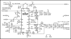
Figure 1. Schematic of the MAX15046 buck power supply at FSW = 250kHz.
Table 1. Bill of Materials
| Designator | Value | Description | Part Number | Manufacturer | Package | Quantity |
| C1 | 470µF/50V | Capacitor | EEVFK1H471M | Panasonic | Electrolytic | 1 |
| C2 | 0.1µF/50V | Capacitor | GRM188R71H104K | Murata | 603 | 1 |
| C3 | 1µF/50V | Capacitor | GRM21BR71H105K | Murata | 805 | 1 |
| C4 | 4.7µF/6.3V | Capacitor | GRM188R60J475K | Murata | 603 | 1 |
| C5 | 2.2µF | Capacitor | GRM188R60J225K | Murata | 603 | 1 |
| C6, C7, C7X | 10µF/50V | Capacitor | GRM55DR70H106K | Murata | 2220 | 3 |
| C8 | 0.47µF/16V | Capacitor | GRM188R71C474K | Murata | 603 | 1 |
| C9 | 2700pF/50V | Capacitor | GRM2165C1H272JA | Murata | 805 | 1 |
| C10 | 470µF/6.3V | Capacitor | EEFSX0D471E4 | Panasonic | 7.3mm x 4.3mm x 1.9mm | 1 |
| C11 | 100µF/6.3V | Capacitor | GRM32ER60J107ME20L | Murata | 1210 | 1 |
| C12 | 100µF/6.3V | Capacitor | GRM32ER60J107ME20L | Murata | 1210 | 1 |
| C13 | 68pF/50V | Capacitor | GRM1885C1H680J | Murata | 603 | 1 |
| C14 | 100pF/50V | Capacitor | GRM39COG101J50D500 | Murata | 603 | 1 |
| C15 | 10nF/50V | Capacitor | GRM188R71H103KA01D | Murata | 603 | 1 |
| C16 | 820pF/50V | Capacitor | GRM39COG821J50D500 | Murata | 603 | 1 |
| C17 | Open | Capacitor | ||||
| C18 | 22µF/6.3V | Capacitor | GRM31CR70J226KE19L | Murata | 1206 | 1 |
| C19 | 1µF/6.3V | Capacitor | GRM188R70J105KA01D | Murata | 603 | 1 |
| R3 | 10Ω | Resistor | Resistor | Multisource | 603 | 1 |
| R4 | 51kΩ | Resistor | Resistor | Multisource | 603 | 1 |
| R5 | 2.2Ω | Resistor | Resistor | Multisource | 603 | 1 |
| R7 | 1Ω | Resistor | Resistor | Multisource | 603 | 1 |
| R8 | Open | Resistor | ||||
| R9 | 19.1kΩ | Resistor | Resistor | Multisource | 603 | 1 |
| R10 | 6.04kΩ | Resistor | Resistor | Multisource | 603 | 1 |
| R11 | 4kΩ | Resistor | Resistor | Multisource | 603 | 1 |
| R12 | 86.6kΩ | Resistor | Resistor | Multisource | 603 | 1 |
| R13 | 86.6kΩ | Resistor | Resistor | Multisource | 603 | 1 |
| R14 | 68.1kΩ | Resistor | Resistor | Multisource | 603 | 1 |
| R15 | 49.9Ω | Resistor | Resistor | Multisource | 603 | 1 |
| R16 | 0 | Resistor | Resistor | Multisource | 603 | 1 |
| R17 | 0 | Resistor | Resistor | Multisource | 603 | 1 |
| L1 | 2.2µH/20A | Inductor | IHLP5050EZER2R2M01 | Vishay | 13.20mm x 12.90mm x 5.00mm | 1 |
| N1 | 60V, 6.2A | n-Channel MOSFET | SI7850DP | Vishay | PowerPAK® SO-8 | 1 |
| N2 | 60V, 18.5A | n-Channel MOSFET | SI7478DP | Vishay | PowerPAK SO-8 | 1 |
| D1 | 0.5A, 60V | Schottky diode | ZHCS506TA | Zetex | SOT23 | 1 |
| U1 | MAX15046 | PWM Controller | MAX15046 | Maxim | 16 PIN TQFN | 1 |
Performance Characteristics
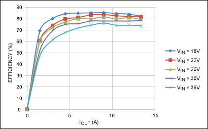
Figure 2. Total system efficiency versus load current relative to different input voltages.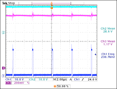
Figure 3. Steady-state input voltage, output voltage, and gate signal.
Ch1: Switching-Node Voltage
Ch2: Input Voltage
Ch3: Output Voltage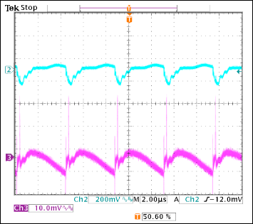
Figure 4. Steady-state peak-to-peak input ripple and peak-to-peak output ripple.
Ch2: Input-Voltage Ripple
Ch3: Output-Voltage Ripple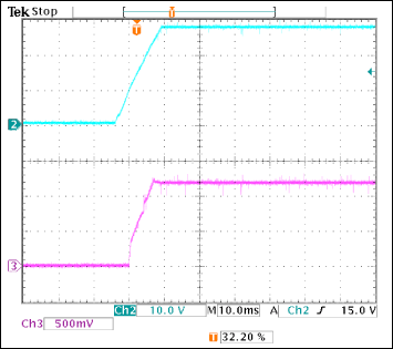
Figure 5. Soft-start when VIN = 28V is applied with a 13.4A load.
Ch2: Input Voltage
Ch3: Output Voltage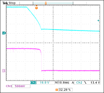
Figure 6. Soft-stop when input power is off.
Ch2: Input Voltage
Ch3: Output Voltage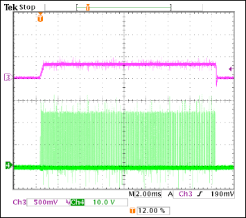
Figure 7. Output voltage and gate signal when the load is short circuited.
Ch3: Output Voltage
Ch4: Gate Signal of High-Side Switch
Board Layout
More detailed image (PDF, 4.7MB)
Figure 8. Two-layer layout of the reference design using the MAX15046 step-down power supply.