Infineon公司的TLE9845QX系列产品是集成了32位ARM? Cortex? M0内核的继电器驱动芯片,MCU工作频率高达40MHz.器件在单个芯片上集成了通过继电器或PN MOSFET半桥来检测,控制和启动电机所需的所有功能,包括48KB闪存,4KB EEPROM,768B 100TP存储器,4KB RAM以及引导ROM,具有高集成度和高性价比.主要用在汽车的电机控制应用如车窗升降器,雨刮,汽车天窗,风扇和风机等.本文介绍了TLE9845QX主要特性,框图,电源管理单元框图,统控制单元-数字模块框图和Cortex-M0框图,以及TLE984x评估板主要特性,框图,电路图,材料清单,PCB元件布局图和设计图.
This highly integrated circuit contains analog and digital functional blocks. For system and interface control anembedded 32-Bit Cortex-M0 microcontroller is included. For internal and external power supply purposes, on-chiplow drop-out regulators are existent. An internal oscillator (no external components necessary) provides a costeffective and suitable clock in particular for LIN slave nodes. As communication interface, a LIN transceiver andseveral High Voltage Monitor Inputs with adjustable threshold and filters are available. Furthermore two High-Sides Switches (e.g. for driving LEDs or powering of switches), two low-side switches (e.g. for relays) and severalgeneral purpose input/outputs (GPIO) with pulse-width modulation (PWM) capabilities are available.
The Micro Controller Unit supervision and system protection including reset feature is controlled by aprogrammable window watchdog. A cyclic wake-up circuit, supply voltage supervision and integrated temperaturesensors are available on-chip.
All relevant modules offer power saving modes in order to support terminal 30 connected automotive applications.
A wake-up from the power saving mode is possible via a LIN bus message, via the monitoring inputs or repetitivewith a programmable time period (cyclic wake-up).
The integrated circuit is available in a package with 0.5 mm pitch and is designed to withstand the challengingconditions of automotive applications.
The TLE9845QX has several operational modes mainly to support low power consumption requirements.
TLE9845QX主要特性:
? 32-bit ARM Cortex-M0 Core
– up to 40 MHz clock frequency
– one clock per machine cycle architecture
– single cycle multiplier
? On-chip memory
– 48 KB Flash (including EEPROM)
– 4 KB EEPROM (emulated in Flash)
– 768 bytes 100 Time Programmable Memory (100TP)
– 4 KB RAM
– Boot ROM for startup firmware and Flash routines
? On-chip OSC
? 2 Low-Side Switches incl. PWM functionality, can be used e.g. as relay driver
? 2 High-Side Switches with cyclic sense option and PWM functionality, e.g. for supplying LEDs or switch panels(min. 150 mA)
? 5 High Voltage Monitor Input pins for wake-up and with cyclic sense with analog measurement option
? 10 General-purpose I/O Ports (GPIO)
? 6 Analog input Ports
? 10-Bit A/D Converter with 6 analog inputs + VBAT_SENSE + VS + 5 high voltage monitoring inputs
? 8-Bit A/D Converter with 7 inputs for voltage and temperature supervision
? Measurement unit with 12 channels together with the onboard 10-Bit A/D converter and data post processing
? 16-Bit timers - GPT12, Timer 2 and Timer 21
? Capture/compare unit for PWM signal generation (CCU6)
? 2 full duplex serial interfaces (UART1, UART2), UART1 with LIN support
? 2 synchronous serial channels (SSC1, SSC2)
? Usage as P/N-channel Power MOSFET driver (Half Bridge Application) supported by four additional differentialchannels in ADC1
? On-chip debug support via 2-wire SWD
? LIN Bootstrap loader to program the Flash via LIN (LIN BSL)
? 1 LIN 2.2 transceiver
? Single power supply from 3.0 V to 28 V
? Low-dropout voltage regulators (LDO)
? 5 V voltage supply VDDEXT for external loads (e.g. Hall-sensor)
? Core logic supply at 1.5 V
? Programmable window watchdog (WDT1) with independent on-chip clock source
? Power saving modes:
– Micro Controller Unit slow-down mode
– Sleep Mode with cyclic sense option
– Cyclic wake-up during Sleep Mode
– Stop Mode with cyclic sense option
? Power-on and undervoltage/brownout reset generator
? Overtemperature protection
? Short circuit protection for all voltage regulators and actuators (High Side, Low Side)
? Loss of clock detection with fail safe mode for power switches
? Temperature Range TJ: -40 °C up to 150 °C
? Package VQFN-48-31 with LTI feature
? Green package (RoHS compliant)
? AEC Qualified
?
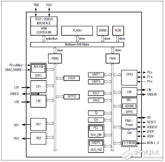
图1.TLE9845QX框图
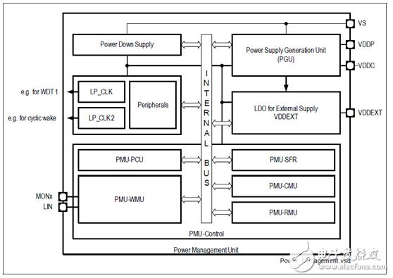
图2.TLE9845QX电源管理单元框图
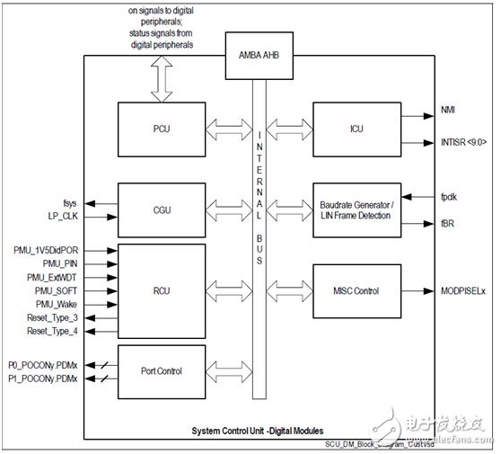
图3.TLE9845QX系统控制单元-数字模块框图
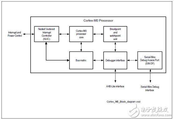
图4.TLE9845QX Cortex-M0框图
TLE984x评估板
The TLE984x Evaluation Board offers complete evaluation of all functions and peripherals of the TLE984x product family.This board is designed to provide a fast and easy start of evaluation, for Infineons embedded Power TLE984xdevice family.
The TLE984x device is placed in the center of the PCB. A socket provides the possibility to test and evaluate all ICsout of the TLE984x device family. Every pin of the IC is connectable via rows of pinheader. The board is protectedagainst reverse polarity of input voltage supply. A bidirectional relay can be connected to the integrated lowsideswitches, optionaly. In addition to that, a scew-connector is placed near the relay to contact and drive a DCmotor(example: window lift motor).
The evaluationboard provides an on board debugger. It is placed in the upper left of Figure 1. It provides a SWDDebugconnection and a virtual COM port for serial UART communication.
Highside and Lowside switches and VDDEXT are connectable via 4mm standard laboratory wires.
The High-Voltage-Monitor pins can be triggered with dedicated pushbuttons.
For analog input values a potentiometer is connected to PIN P2.2.
The LIN connection is able to be configured to master and slave mode.
?
图5.TLE984x评估板外形图
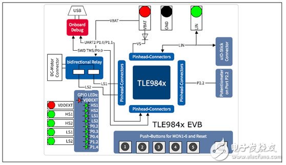
图6.TLE984x评估板框图
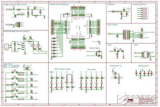
图7.TLE984x评估板电路图(1)
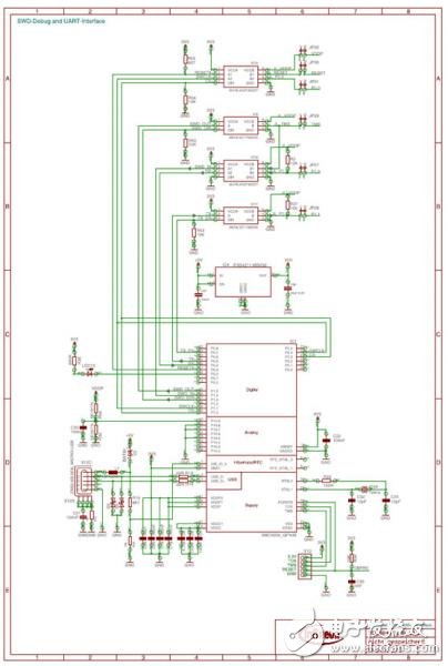
图8.TLE984x评估板电路图(2)
TLE984x评估板材料清单:
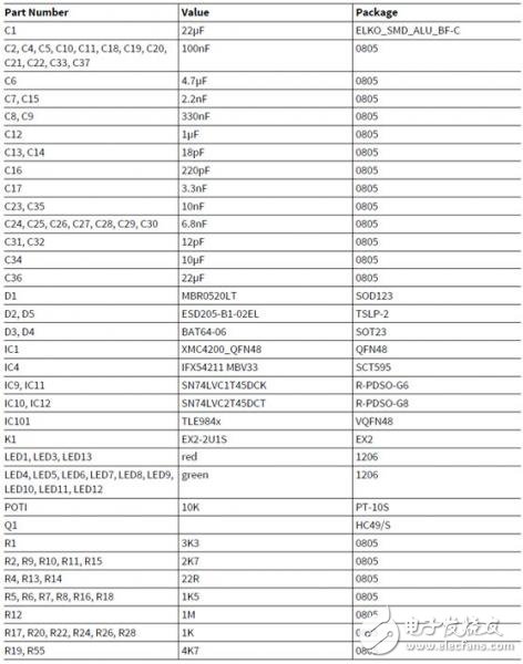
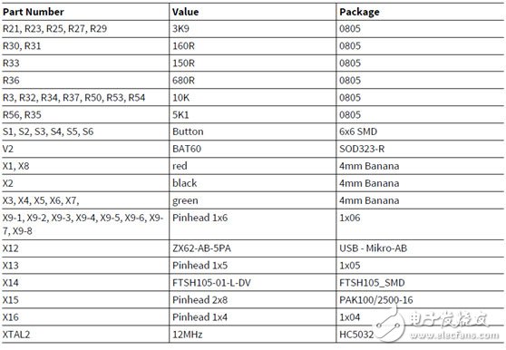
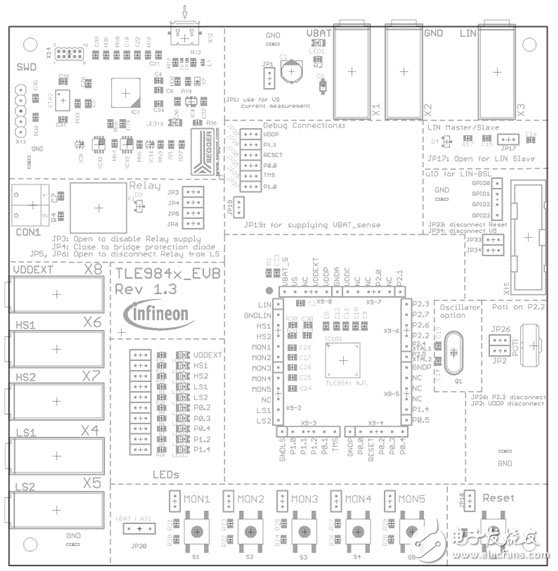
图9.TLE984x评估板PCB元件布局图
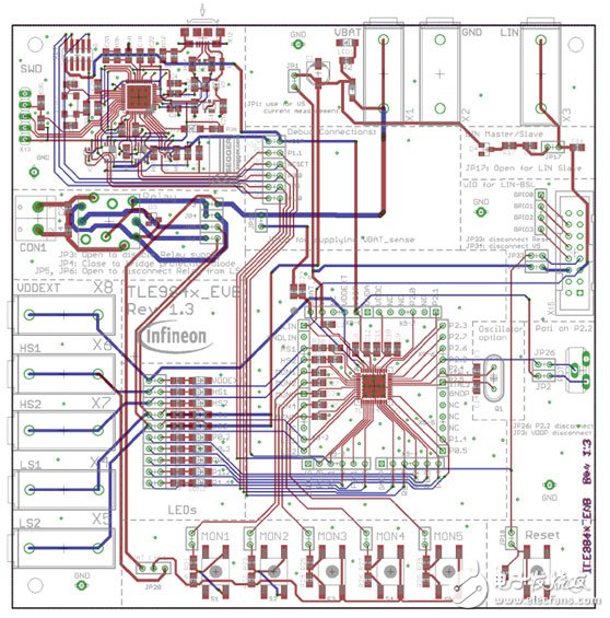
图10.TLE984x评估板PCB布局图