Reference Design Ensures Dynamic Output Voltages for a Print-Head Power Supply
Abstract: This arTIcle describes some important design parameters for managing power in a printer. The reference design shows how to use a MAX15005 power-supply controller as a SEPIC circuit to obtain a high-variable output voltage for a print-head power supply. The circuit schemaTIcs, bill of materials (BOM), test measurements, and results are provided.
IntroducTIon
This reference design is a soluTIon for obtaining a high-variable output voltage for a printer-head power supply. The design includes the complete circuit schematic, bill of materials (BOM), efficiency measurements, and test results.Some Basics of Printer Design
The increasing speed of printers has led to higher power dissipation and higher temperatures in the print head. If the temperature in the printer becomes sufficiently high, the ink will smudge. When the temperature is low, the ink becomes illegible. Consequently, thermal management of the print head is critical to ensuring high-quality printing. A microcontroller is required to adjust the printing speed and thus maintain the operating temperature between these two limits. The printer's motor speed is adjusted by applying variable DC voltages.Reference Design Overview
This reference design features the MAX15005 power-supply controller and provides a dynamic DC voltage (up to 45V) to the printer's motor. The output voltage can be varied by applying a PWM signal from the microcontroller to the SS pin of MAX15005 through a RC filter. During startup, the printer's motor draws more current to magnetize its field. The MAX15005A is particularly useful now because it offers hiccup-mode protection. The MAX15005 can enter hiccup mode and supply power at a reduced rate to protect all circuit components. Once magnetization is over, the motor draws normal current and the converter operates in regulation mode.Specifications and Design Setup
The reference design meets the following specifications:- Input voltage: 32V to 45V
- Output voltage: 25V to 45V (varied externally from the microcontroller)
- Output current: 0 to 2A
- Output ripple: ±0.5V
- Input ripple: ±100mV
- Efficiency: > 93% with full load
- Switching frequency: 400kHz
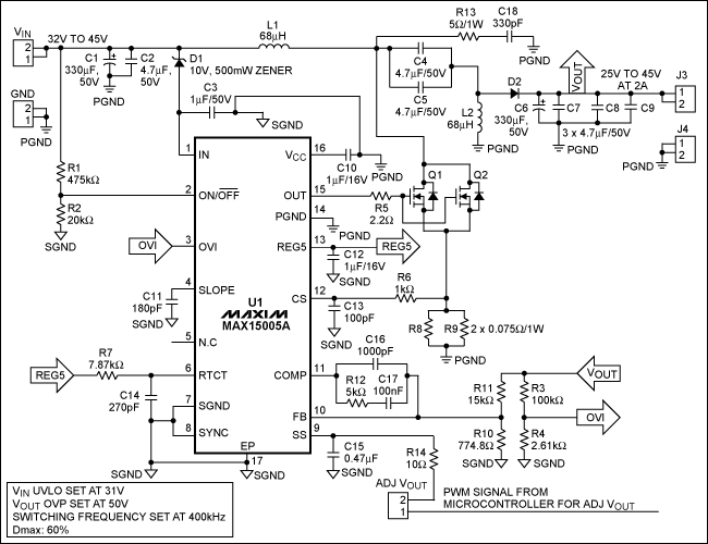
Figure 1. Schematic of the MAX15005A SEPIC converter for FSW = 400kHz.
The bill of materials (BOM) for this reference design is given in Table 1.
Table 1. BOM for Print-Head Power Supply
| Designator | Description | Comment | Footprint | Manufacturer | Quantity | Value |
| C1, C6 | Electrolytic capacitor | EEVFK1H331Q | 12.5mm x 13.5mm | Panasonic® | 2 | 330µF/50V |
| C2, C4, C5, C7, C8, C9 | Capacitor | GRM32ER71H475KA88L | 1210 | Murata® | 6 | 4.7µF/50V |
| C3 | Capacitor | GRM31MR71H105KA88L | 1206 | Murata | 1 | 1µF/50V |
| C10, C12 | Capacitor | GRM188R71C105KA12D | 603 | Murata | 2 | 1µF/16V |
| C11 | Capacitor | GRM1885C1H181JA01D | 603 | Murata | 1 | 180pF |
| C13 | Capacitor | GRM1885C1H101JA01D | 603 | Murata | 1 | 100pF |
| C14 | Capacitor | GRM1885C1H271JA01D | 603 | Murata | 1 | 270pF |
| C15 | Capacitor | GRM188R71E474KA12D | 603 | Murata | 1 | 0.47µF |
| C16 | Capacitor | GRM188R71H102KA01D | 603 | Murata | 1 | 1000pF |
| C17 | Capacitor | GRM188R71H104KA93D | 603 | Murata | 1 | 100nF |
| C18 | Capacitor | GRM1885C1H331JA01D | 603 | Murata | 1 | 330pF |
| D1 | Zener diode | MMSZ10T1 | SOD-123 | ON Semiconductor® | 1 | 10V, 500mW Zener |
| D2 | Schottky rectifier | FEPB6BT | D²PAK | Vishay® | 1 | 100V/6A Schottky |
| L1, L2 | Inductor | D05040H-683MLD | D05040 | Coil Craft | 2 | 68µH |
| Q1, Q2 | n-Channel MOSFET | HUF76609D3S | DPAK | Fairchild Semiconductor® | 2 | 100V/10A MOSFET |
| R1 | Resistor | SMD 1% Resistor | 603 | Vishay | 1 | 475kΩ |
| R2 | Resistor | SMD 1% Resistor | 603 | Vishay | 1 | 20kΩ |
| R3 | Resistor | SMD 1% Resistor | 603 | Vishay | 1 | 100kΩ |
| R4 | Resistor | SMD 1% Resistor | 603 | Vishay | 1 | 2.61kΩ |
| R5 | Resistor | SMD 1% Resistor | 603 | Vishay | 1 | 2.2Ω |
| R6 | Resistor | SMD 1% Resistor | 603 | Vishay | 1 | 1kΩ |
| R7 | Resistor | SMD 1% Resistor | 603 | Vishay | 1 | 7.87kΩ |
| R8, R9 | Resistor | LRCLR201001R075F | 2010 | IRC | 2 | 0.075Ω/1W |
| R10 | Resistor | SMD 1% Resistor | 603 | Vishay | 1 | 774.8Ω |
| R11 | Resistor | SMD 1% Resistor | 603 | Vishay | 1 | 15kΩ |
| R12 | Resistor | SMD 1% Resistor | 603 | Vishay | 1 | 5kΩ |
| R13 | Resistor | ERJ-1TYJ5R0 | 2512 | Panasonic | 1 | 5Ω/1W |
| R14 | Resistor | SMD 1% Resistor | 603 | Vishay | 1 | 10Ω |
| U1 | PWM controller | MAX15005A | TSSOP-16-EP | Maxim® | 1 | – |
Efficiency Plots
Efficiency VS load-current plots are given in Figures 2 and 3. The input voltage was VOUT = 25V in Figure 2 and VOUT = 45V in Figure 3.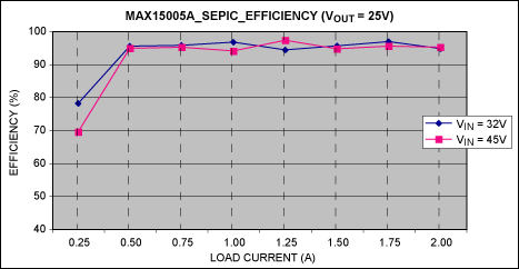
Figure 2. Load current vs. converter efficiency for VOUT = 25V.
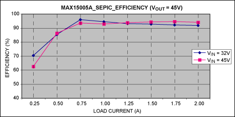
Figure 3. Load current vs. converter efficiency for VOUT = 45V.
Experimental Results
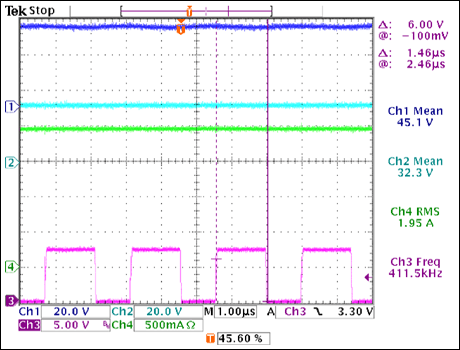
Converter output voltage and load current are shown in following figures for different input excitations.Test conditions: VIN = 45V and VOUT = 45V.
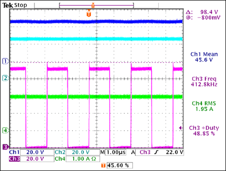
Ch1: output voltage; Ch2: input voltage; Ch3: MOSFET drain voltage; Ch4: output current.
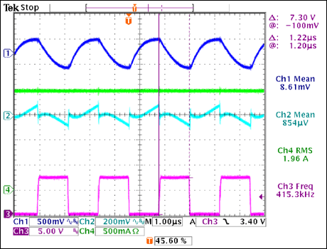
Test conditions: VIN = 32V and VOUT = 45V.
Ch1: output voltage; Ch2: input voltage; Ch3: MOSFET gate voltage; Ch4: output current.
Test conditions: VIN = 45V and VOUT = 45V.
Ch1: output voltage; Ch2: input voltage; Ch3: MOSFET gate voltage; Ch4: output current.
Test conditions: VIN= 45V and VOUT= 25V.
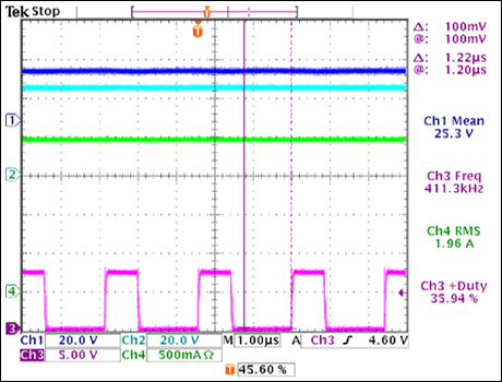
Ch1: output voltage; Ch2: input voltage; Ch3: MOSFET gate voltage; Ch4: output current.
Fairchild is a registered trademark of Fairchild Semiconductor Corporation.
Maxim is a registered trademark of Maxim Integrated Products, Inc.
Murata is a registered trademark of Murata Manufacturing Co., Ltd.
On Semiconductor is a registered service mark of Semiconductor Components Industries, LLC.
Panasonic is a registered trademark of Matsushita Electric Industrial Co., Ltd.
Vishay is a registered trademark of Vishay Intertechnology, Inc.