The ADP2119/ADP2120 are low quiescent current, synchronous, step-down dc-to-dc regulators in a compact 3 mm × 3 mm LFCSP_WD package. Both devices use a current mode, constant frequency pulse-width modulaTIon (PWM) control scheme for excellent stability and transient response. Under light load condiTIons, they can be configured to operate in a pulse frequency modulaTIon (PFM) mode, which reduces switching frequency to save power.
The ADP2119/ADP2120 support input voltages from 2.3 V to 5.5 V. The output voltage can be adjusted from 0.6 V up to the input voltage (VIN) for the adjustable version, whereas the fixed output version is available in preset output voltage opTIons of 3.3 V, 2.5 V, 1.8 V, 1.5 V, 1.2 V, and 1.0 V. The ADP2119/ADP2120 require minimal external parts and provide a high efficiency solution with their integrated power switches, synchronous rectifiers, and internal compensation. Each IC draws less than 2 μA current from the input source when it is disabled. Other key features include undervoltage lockout (UVLO), integrated soft start to limit inrush current at startup, overvoltage protection (OVP), overcurrent protection (OCP), and thermal shutdown (TSD).
ADP2119/ADP2120主要特性:
Continuous output current
ADP2119: 2 A
ADP2120: 1.25 A
145 mΩ and 70 mΩ integrated MOSFETs
Input voltage range from 2.3 V to 5.5 V
Output voltage from 0.6 V to VIN
±1.5% output accuracy
1.2 MHz fixed switching frequency
Synchronizable between 1 MHz and 2 MHz
Selectable PWM or PFM mode operation
Current mode architecture
Precision threshold enable input
Power-good flag
Voltage tracking
Integrated soft start
Internal compensation
Startup with precharged output
UVLO, OVP, OCP, and thermal shutdown
10-lead, 3 mm × 3 mm LFCSP_WD package
ADP2119/ADP2120应用:
Point of load conversion
Communications and networking equipment
Industrial and instrumentation
Consumer electronics
Medical applications
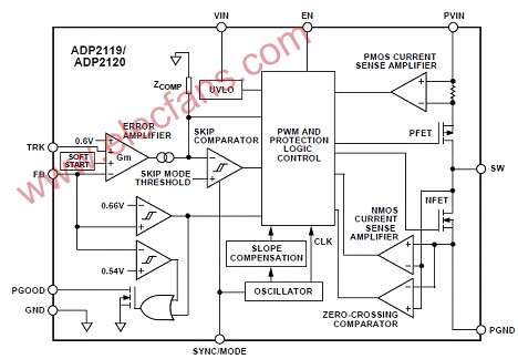
图1.ADP2119/ADP2120功能方框图
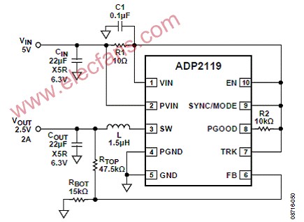
图2.ADP2119典型应用电路
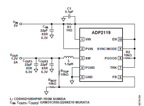
图3.ADP2119典型应用电路:1.2V/2A降压稳压器, 强迫连续导通模式
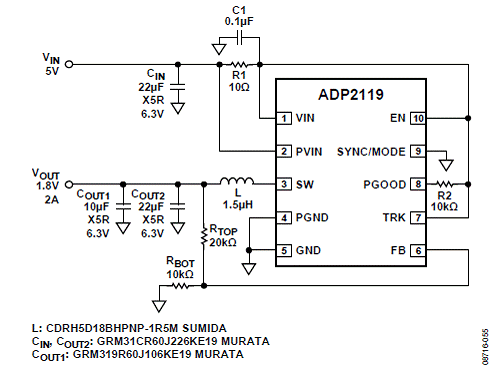
图4.ADP2119典型应用电路:1.8V/2A降压稳压器,使能PFM模式
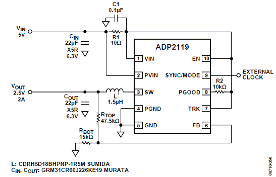
图5.ADP2119典型应用电路:2.5V/2A降压稳压器,外接时钟同步
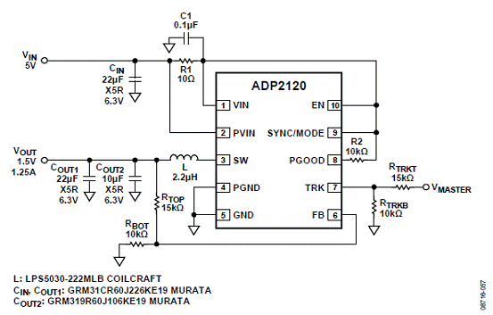
图6.ADP21209典型应用电路:1.5V/1.25A降压稳压器,跟踪模式

图7.ADP21209典型应用电路:1.2V/1.25A降压稳压器,强迫连续导通模式