本文介绍了LM5119主要特性,方框图,典型应用电路图和LM5119EVAL评估板主要特性,电路图和材料清单(BOM)。
NS 公司的LM5119是双路同步电流模式降压控制器,工作电压从5.5V到65V,开关频率从50kHz 到 750kHz,具有强固的3.3A峰值栅极驱动器,可编程输出从0.8V起到输入电压的90%,输出电流高达20A,主要用在需要精密电压稳压器如通信,汽车电子以及工业控制应用。
LM5119主要特性:
■ Emulated peak current mode control
■ Wide operaTIng range from 5.5V to 65V
■ Easily configurable for dual outputs or interleaved single output
■ Robust 3.3A peak gate drive
■ Switching frequency programmable to 750kHz
■ OpTIonal diode emulaTIon mode
■ Programmable output from 0.8V
■ Precision 1.5% voltage reference
■ Programmable current limit
■ Hiccup mode overload protecTIon
■ Programmable soft-start
■ Programmable line under-voltage lockout
■ Automatic switch-over to external bias supply
■ Channel2 enable logic input
■ Thermal Shutdown
■ Leadless LLP32 (5mm x 5mm) package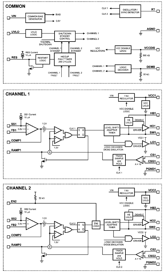
图1。LM5119方框图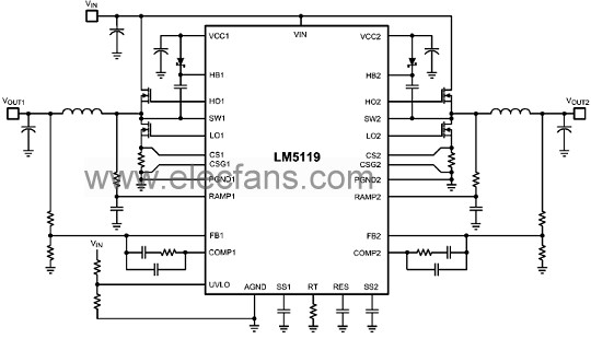
图2。LM5119典型应用电路图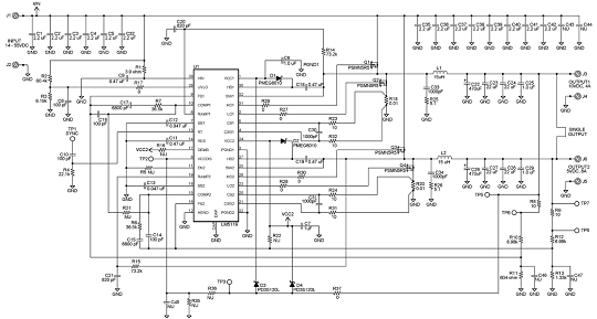
图3。LM5119 10V 4A和5V 8A典型应用电路图
LM5119EVAL评估板
The LM5119EVAL evaluation board provides the design engineer with a fully functional dual output buck converter, employing the LM5119 Dual Emulated Current Mode Synchronous Buck Controller. The evaluation board is designed to provide both 10V and 5V outputs over an input range of 14V to 55V. Also the evaluation board can be easily configured for a single 10V, 8A regulator.
LM5119EVAL评估板主要特性:
Performance of the Evaluation Board
? Input Voltage Range: 14V to 55V
? Output Voltage: 10V (CH1), 5V (CH2)
? Output Current: 4A (CH1), 8A (CH2)
? Nominal Switching Frequency: 230 KHz
? Synchronous Buck Operation: Yes
? Diode Emulation Mode: Yes
? Hiccup Mode Overload Protection: Yes
? External VCC Sourcing: Yes
Powering and Loading Consideration
When applying power to the LM5119 evaluation board, certain precautions need to be followed. A misconnection can damage the assembly.
PROPER BOARD CONNECTION
The input connections are made to the J1 (VIN) and J2 (RTN/ GND) connectors. The CH1 load is connected to the J3 (OUT1+) and J4 (OUT1-/GND) and the CH2 load is connected to the J6 (OUT2+) and J5 (OUT2-/GND). Be sure to choose the correct connector and wire size when attaching the source power supply and the load.
SOURCE POWER
The power supply and cabling must present low impedance to the evaluation board. Insufficient cabling or a high impedance power supply will droop during power supply application with the evaluation board inrush current. If large enough, this droop will cause a chattering condition during power up. During power down, insufficient cabling or a high impedance power supply will overshoot. This overshoot will cause a non-monotonic decay on the output.
An additional external bulk input capacitor may be required unless the output voltage droop/overshoot of the source power is less than 0.7V. In this board design, UVLO setting is conservative while UVLO hysteresis setting is aggressive.
Minimum input voltage can goes down with an aggressive design. Minimum operating input voltage depends on the output voltage droop/overshoot of the source power supply and the forced off-time of the LM5119. Refer to the LM5119 datasheet for complete design information.
LOADING
When using an electronic load, it is strongly recommended to power up the evaluation board at light load and then slowly increase the load. If it is desired to power up the evaluation board at maximum load, resistor banks must be used. In general, electronic loads are best suited for monitoring steady state waveforms.
AIR FLOW
Prolonged operation with high input voltage at full power will cause the MOSFETs to overheat. A fan with a minimum of 200LFM should be always provided.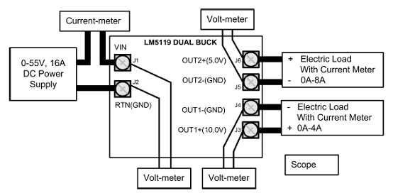
图4。LM5119EVAL评估板连接图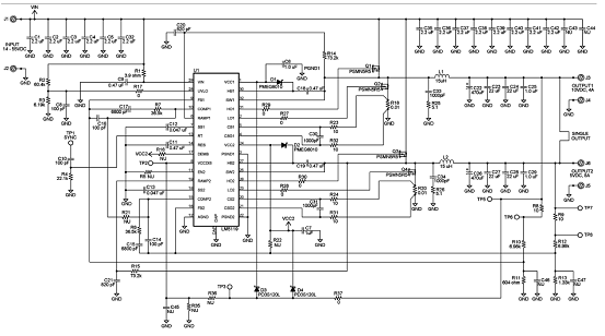
图5。LM5119EVAL评估板电路图
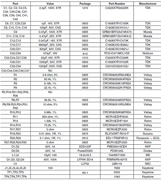
LM5119EVAL评估板材料清单(BOM):