NegaTIve Charge Pumps Achieve Inductor-Like Efficiency for WLED Backlights
Abstract: Designers convenTIonally use boost circuits with capacitor charge pumps or inductors to provide the necessary forward bias for white LEDs (WLEDs). Charge pumps are less expensive and simpler to use, but, unTIl now, they have also been less efficient than inductor-based boost circuits. This applicaTIon note presents a negative-charge-pump design that achieves the efficiency of inductor-based designs while still retaining the simplicity and low cost of an inductorless design.
A similar version of this article was featured in Maxim's Engineering Journal, vol. 64 (PDF, 1.99MB).
Overview
Offering a small footprint and high light output, white LEDs (WLEDs) provide an ideal backlight solution for small color displays in cellular phones and other portable devices. WLEDs, however, do present one difficulty in devices powered from a single-cell lithium-ion (Li+) battery. The operating voltage from most Li+ cells is 3V to 4.2V, while a WLED’s forward voltage is typically 3.5V to 3.8V (at 20mA). Consequently, the voltage output at the lower end of a Li+ battery’s operating range is not enough to bias WLEDs.
Two approaches are commonly used to generate adequate forward bias for WLEDs: capacitor-charge-pump and inductor-based boost circuits. Traditionally, inductor-based circuits have been the best choice for efficiency and battery life. However, they require the addition of that costly inductor, and necessitate careful layout and design to avoid electromagnetic and RF interference issues. In contrast, charge-pump solutions are simpler to implement and cost less, but they have also typically been less efficient, which can reduce battery runtime.
Negative-Charge-Pump Technology Enables Lower-Cost, Energy-Efficient Applications
Maxim’s negative-charge-pump architecture with adaptive switchover enables WLED driver ICs to achieve inductor-like efficiencies (averaging 85%) while still retaining the simplicity and low cost of an inductorless design.
This innovative topology employs adaptive mode-switching technology to supply, dim, and regulate each LED individually. Delivering a 12% increase in LED efficiency, this approach extends battery life and saves valuable PCB real estate in portable applications. By providing efficiency comparable to inductor-based designs, these devices effectively reduce the price point of energy efficiency.
Efficiency Improvements Among Fractional-Ratio Charge Pumps
The first generation of WLED charge-pump solutions used a basic doubler topology (or 2x mode) at its core. The efficiency of a 2x charge pump is:
PLED/PIN = VLED × ILED/[(2 × VIN × ILED + IQ × VIN)]
where IQ is the circuit's quiescent operating current.
Because the IQ is usually small compared to the WLED's load current, the efficiency can be closely approximated by:
PLED/PIN ≈ VLED/2VIN
To improve efficiency, second-generation WLED charge pumps did not always drive the output to a whole multiple of the input. If the battery voltage was sufficient, adequate LED drive voltage could be generated with a 1.5x charge pump. The conversion efficiency of a 1.5x pump is:
PLED/PIN = VLED × ILED/(1.5 × VIN × ILED + IQ × VIN)≈ VLED/1.5VIN
As can be seen, the 1.5x pump substantially improves efficiency. With a 3.6V battery voltage and a 3.7V WLED, efficiency jumps from 51% with a 2x pump to 69% with a 1.5x pump.
Third-generation WLED drivers added further improvement with a 1x transfer mode that connects the battery directly to the LEDs through low-dropout current regulators when the battery voltage is high enough. This efficiency is described by:
PLED/PIN = VLED × ILED/(VIN × ILED + IQ × VIN)
When the battery voltage is sufficient to directly drive WLEDs, 1x mode efficiency can be over 90%. With a 4V battery and a 3.7V WLED, efficiency is 92%.
Maximizing Efficiency at Each Battery Voltage
An optimum WLED driver design employs the most efficient power-transfer mode possible for a given battery and LED voltage. The design also changes modes as the battery (or WLED) voltage changes. However, switch losses can force the circuit into a less efficient mode at a higher battery voltage than might otherwise be necessary. It is always best for the driver to stay in a high-efficiency mode as long as possible while the battery voltage falls. However, this performance requires minimum loss in the power switches and, consequently, more space and cost.
As noted above, the best conversion efficiency is offered by a 1x transfer mode, but this mode can only be used when the battery voltage is more than the WLEDs’ forward voltage (VF). The key to utilizing 1x mode for the lowest possible battery voltage has usually focused on lowering both the voltage drop of the 1x mode bypass FET and that of the current regulator. These voltage drops determine the series losses and minimum input voltage that can sustain 1x mode. The minimum battery voltage required by 1x mode is:
VIN(MIN_1X) = VLED + bypass pFET RDS(ON) × (ILED + VDROPOUT of the current regulator)
A traditional positive-charge-pump WLED solution uses a pFET bypass switch to connect the battery voltage to the WLEDs, as shown in Figure 1. This FET’s RDS(ON) is typically 1Ω to 2Ω. Further resistance reductions are limited since lower resistances typically would necessitate a larger FET, increasing the cost of the power device. 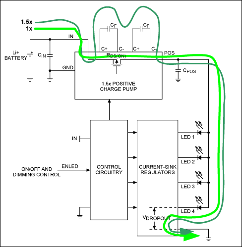
Figure 1. In 1x mode, the positive charge pump uses an internal switch to bypass VIN to the WLEDs' anodes.
A positive charge pump generates 1.5x VIN or 2x VIN to drive the WLED anodes when VIN is insufficient to drive a 1x transfer mode. To implement the 1x mode in a positive-charge-pump architecture, we must use an additional internal switch to route VIN directly to the WLEDs’ anodes, thereby bypassing the charge pump.
A negative-charge-pump architecture also generates -0.5x VIN to drive WLED cathodes when VIN is insufficient for the task. This architecture, however, does not require that you bypass the -0.5x VIN charge-pump output to ground in 1x mode because current regulators control the WLEDs’ current directly from VIN to ground. As a result, the negative-charge-pump architecture extends 1x mode all the way down t
VIN(MIN_1X) = VLED + VDROPOUT of the current regulator
Figure 2 shows the current path of 1x mode with a negative charge pump. The circuit does not require a pMOS bypass switch, and it directly regulates WLED current from VIN to ground. If ILED is 100mA total (i.e., 5 WLEDs × 20mA), a 2Ω pMOS bypass switch’s voltage drop would be 200mV. As it discharges, the Li+ battery voltage holds relatively stable around the 3.6V to 3.8V (typical) voltage range. Assuming a typical Li+ battery-discharge curve, the 200mV increase in operating voltage enabled by 1x mode dramatically improves efficiency.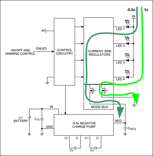
Figure 2. Individual switchover for each WLED is possible when the driver switches to its negative-charge-pump mode, which improves overall efficiency
Maximizing Efficiency at Each LED Forward Voltage
In a traditional 1x/1.5x positive-charge-pump WLED driver, the WLED anodes connect to the charge pump’s output. If the WLEDs are mismatched, the driver must switch to 1.5x mode when there is not enough (VIN - VLED) headroom to support the worst forward-voltage WLED.
With the negative-charge-pump architecture, it is no longer necessary to abandon the efficient 1x mode due to the bad forward voltage of only one WLED. As Figure 2 illustrates, the Mode Mux circuit individually selects 1x mode or -0.5x mode for each WLED, thereby maximizing overall efficiency.
The MAX8647/MAX8648 charge-pump drivers, for example, turn on the -0.5x charge pump when the input voltage is insufficient to drive the highest forward-voltage WLED. In this situation, the devices drive only the highest VF WLED through the -0.5x negative rail (instead of ground), while the WLEDs with lower forward voltages remain in 1x mode.
To further improve efficiency, the MAX8647/MAX8648 provide individual mode switching for the WLEDs. This technology adaptively switches the WLEDs to -0.5x mode at different times and at different VIN levels due to VF mismatches or temperature changes (Figure 3).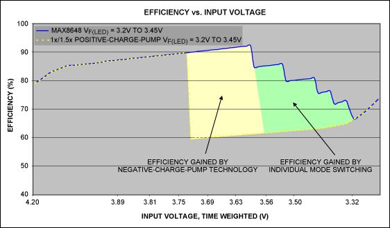
Figure 3. The efficiency of the MAX8647/MAX8648 charge-pump WLED drivers can be extended by switching to a negative-charge-pump mode and to individual mode switching for each WLED
Summary
Traditionally, WLED backlight designs that employ charge pumps have been less efficient than inductor-based designs. A positive-charge-pump architecture switches from its highest efficiency mode (1x) when any single WLED current falls below a predetermined level. Thus, systems with a large number of WLEDs and large forward-voltage mismatch waste a significant amount of power.
A negative-charge-pump architecture overcomes the inefficiencies typically encountered in positive-charge-pump designs. Devices such as the MAX8647/MAX8648 use this negative-charge-pump architecture, as well as individual mode switching for each LED, to dramatically improve efficiency and extend battery runtime. These WLED drivers enable designers to achieve inductor-like efficiencies while benefiting from the simplicity and cost savings offered by charge-pump solutions.
A similar version of this article appeared in Korean in the May 2008 issue of Semiconductor Network.