Buck Regulator Generates Ultra-Low Output Voltage
Abstract: You can induce a switching regulator to produce a regulated output lower than its internal reference voltage by adding a higher-voltage external reference.
IC processes with lower voltages are increasing the need for efficient sub-1.25V supply voltages. Many switching regulators employ a 1.25V reference, making it difficult to supply less than 1.25V. Under the right set of circumstances, however, the limitaTIon vanishes, allowing the regulator to generate output voltages well below that of the feedback pin.
The first requirement is another regulated voltage (Ref2) higher than the buck regulator's feedback voltage (VFB), and accurate enough to serve as an addiTIonal reference. It can come from a voltage-reference IC such as IC2 in Figure 1, from another precision reference such as those built into many ADCs, or (for lower-accuracy applicaTIons) a low-dropout linear regulator (LDO) with 1% tolerance. The current drawn from Ref2 is small, so any of these opTIons is acceptable. Note that for any source other than the stand-alone reference dedicated to this circuit, loading from other unrelated circuitry is a potential noise source that can degrade the power converter's noise performance. Decoupling may be required.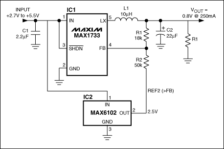
Figure 1. A voltage reference with 2.5V output (IC2) allows the buck regulator (IC1) to produce an output voltage of 0.8V.
The second requirement is simply a small minimum load on the regulator output sufficient to maintain the desired output voltage in all cases, while also sinking current from the two voltage-setting resistors. Instead of connecting the bottom of the lower resistor to ground, tie it to Ref2. Current then flows in the opposite direction through R2 (because Ref2 > VFB), causing the output to be lower than VFB (Figure 1). Pick the R1/R2 ratio as usual, noting that the current in R2 [(Ref2-VFB)/R2] also flows through R1 to the output:
VOUT = 1.25V - R1(Ref2-VFB)/R2.
These circuit connections should have no adverse effect on stability if Ref2 is electrically quiet. Otherwise, you should add noise-filtering components close to the converter. Any required loop compensation should be identical to that of a standard application with ground-based voltage setting.
The Ref2 voltage should not be higher than the dc-dc converter's minimum input voltage. If the converter is turned off when Ref2 is present and the load is disconnected, the converter's FB and LX pins are driven to the reference voltage, and a reference higher than the converter's input voltage violates the voltage limitation on those pins. A reference IC may not generate enough current to damage IC1, but a large LDO might. That condition is easily avoided with a lower value for Ref2.