Display BacklighTIng Using High-Brightness LEDs and SEPIC Power Modules
Abstract: In automoTIve applicaTIons, offering a wide dimming raTIo for backlights is important because the display panel must be viewable in both direct sunlight and in complete darkness. The latest high-brightness (HB) LEDs offer a backlighting solution that provides a wider dimming ratio, better reliability, and lower power consumption than CCFLs. SEPIC power converters provide a flexible and power-efficient solution for driving strings of HB LEDs, while permitting a wide, 4000:1 dimming ratio. This article discusses the use of SEPIC power modules and the MAX16807/MAX16808 HB LED drivers to deliver a wide-dimming-ratio backlight solution.
Overview
In the automotive industry, designers have begun replacing cold-cathode fluorescent lamps (CCFLs) with high-brightness LEDs (HB LEDs) for backlighting automotive display panels such as navigation and infotainment systems. As compared to CCFLs, HB LEDs operate at lower DC voltages (implying less EMI), have a longer life, perform much better in extreme temperature and vibration environments, do not contain mercury, and provide "instant on" operation. Furthermore, while CCFLs are limited to 300:1 dimming ratios (at best), HB LEDs can have dimming ratios of 4000:1 or higher.
Wide dimming ratios are particularly important in cars because they are subject to a severe ambient-light range. In direct sunlight, the backlight intensity must be great enough to resist washout. At night, the display must reduce the backlight intensity significantly so that it does not interfere with the driver's vision. Because of the need for uniformity, backlights usually employ multiple strings of HB LEDs and arrange them in a matrix formation. Serial strings provide the advantage of supplying all the HB LEDs with the same current, assuring that the intensity and spectral content is consistent. To guarantee consistency between strings, designs usually require accurate current drivers.
Conventional Design Challenges of HB LED Drivers
While achieving a wide dimming ratio may seem trivial, it presents some tough problems when you have to consider efficiency needs. Pulse-width modulating (PWM) linear HB LED drivers at a frequency of 250Hz or higher can do the job. However, these linear drivers dissipate copious amounts of power, and heat removal can become a difficult challenge. The obvious solution to poor efficiency is to employ switch-mode HB LED drivers. Unfortunately, switcher magnetics and control circuits have a difficult time responding to the very short on times that 4000:1 PWMing would require (a 0.025% duty cycle with a 250Hz frequency is equal to 1µs).
A reasonable solution to this problem is a combination of an adaptive switching regulator and linear drivers. An adaptive switcher does not deliver a fixed voltage. Instead, it trims the output voltage to be very close to the stack voltage of the particular HB LED string with the highest series voltage. The switching regulator achieves this by "diode ORing" the drain voltages of the drivers, and selecting the lowest value to regulate. The linear drivers then provide fast PWMing of the individual HB LED strings.
This hybrid approach reduces the power dissipation to a tolerable level and yet allows for very short on times. However, a complication exists whenever the HB LEDs are turned off (PWM = low) and the power-supply adaptive feedback loop loses its sensing voltage. The control loop would normally react to the off mode by allowing the HB LED source voltage to collapse, which is not satisfactory for very low duty cycles. Therefore, the switching regulator must have a "resting" mode at a voltage high enough to guarantee proper operation of short duty cycle "on" pulses and give the regulator time to recover for longer pulses.
Advantages of SEPIC Designs
The number of HB LEDs in series usually varies with the application, and their forward voltages typically have a ±15% tolerance. Also, in automotive environments, the input voltage normally has a fairly large range. Because of these uncertainties, single-ended primary inductance converter (SEPIC) designs are often the switching-regulator topology of choice. SEPICs enhance flexibility because they allow the input to be greater than or less than the output voltage. On the downside, SEPICs require two inductors (or a coupled inductor) and a series blocking capacitor. However, compared to their main competition—flybacks—SEPICs have an advantage in that the series capacitor absorbs any energy stored in leakage inductance, reducing stress on the switching MOSFET.
In the example shown in Figure 1 and Figure 2, a MAX16807 provides the central controller in a SEPIC design that supplies 150mA to two 5-HB LED strings. The IC uses peak-current-mode control and allows for a variable switching frequency. Furthermore, the MAX16807 has eight programmable current sinks, each with a 50mA, 36V driver that accurately sets the current in the strings. You can connect the outputs together for higher currents. The active-low OE pin can turn the HB LED drivers on and off with very short duty cycles, allowing for a wide dimming ratio. The MAX16807 presents a nice combination of features in which the IC controls a SEPIC power supply, creates a common voltage, and then regulates the current in each of those strings with linear drivers.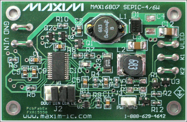
Figure 1. Example of a SEPIC design that drives two 5-HB LED strings at 150mA per string.![Figure 2. Schematic for the Figure 1 circuit using the MAX16807 SEPIC LED driver (VIN = 8V to 18V, VLED = 22V [adaptive], ILED = 150mA/string).](/img/20200428/200926121539795.gif)
More detailed image (PDF, 90.7KB)
Figure 2. Schematic for the Figure 1 circuit using the MAX16807 SEPIC LED driver (VIN = 8V to 18V, VLED = 22V [adaptive], ILED = 150mA/string).
Analysis of the SEPIC Design
In a SEPIC design, there is a primary inductor (L1), a secondary inductor (L2), and a series capacitor (C3), which sits between the two inductors. In some ways, you can think of a SEPIC as a boost regulator with a DC blocking cap to eliminate the input voltage, thus allowing the output to go above or below the input. However, in order to reset that blocking cap and allow energy to flow to the output, a second inductor (L2) is placed on the secondary side.
By analyzing the circuit, you can see that the DC voltage on C3 is equal to the input voltage. When the MOSFET Q1 is turned on, VIN charges L1 and C3 charges L2. Since the voltage on C3 equals the input voltage, the same charging voltage is applied to each inductor during the on time. Also, during the off time, each inductor sees the same discharge voltage—the output voltage plus the D1 forward voltage. Because L1 and L2 have the same charge and discharge voltage, they can have the same inductance and their ripple currents are the same, but their average currents are quite different.
When Q1 is on, D1 is reverse biased and only the output cap C12 supports the output current (ILED). When Q1 is off, inductor current in L1 flows through C3 and combines with the current in L2 to recharge the output capacitor and support ILED. By studying the equations, you will find that basically the current in L2 supports ILED, and the current in L1 recharges the output cap. That means that the L2 average current is equal to ILED, but the L1 average current is equal to ILED × VOUT/VIN.
To get help in the selection of SEPIC components, use the SEPIC Design Spreadsheet, which can be downloaded.
Selecting an Operating Frequency
Selecting an operating switching frequency requires balancing the need to minimize the inductor and capacitor sizes without placing undue thermal stress on Q1 with high switching frequencies. The MAX16807 data sheet provides a formula to determine the switching frequency using a timing resistor (R6) and a timing capacitor (C7). With a 3kΩ resistor and a 1000pF capacitor, the power supply will have a nominal frequency of 500kHz, which seems to be a satisfactory compromise between size and efficiency.
Current Sensing
The MAX16807 is a peak-current-mode controller. Peak current mode compares the peak switch current to an error voltage derived from the output voltage to create a duty cycle and control the output voltage. This same current sense provides overcurrent protection. To reduce the incidence of nuisance trips, the circuit employs a 100ns filter comprising R7 (1kΩ) and C10 (100pF). This filter is large enough to eliminate voltage spikes, and yet it does not distort the current waveform excessively.
Slope Compensation
Subharmonic instability occurs with current-mode control if the duty cycle ever exceeds 50%. This is due to the upward (on) current slope being less than the downward (off) current slope. The instability manifests itself as an alternating large/small duty cycle as the regulator hunts for the correct duty cycle. The instability can increase ripple currents and voltages. To eliminate this problem, an additional, injected artificial slope augments the current-sense signal.
The base of transistor Q2 connects to the ramp voltage present on the RTCT pin. This ramp drives Q2 into D2 and R8 to provide a small current in R7, which effectively adds the slope compensation to the actual sensed current signal. Figure 3 shows the basic slope-compensation signal, the current-sense signal, and the filtered sum of the two.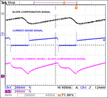
Figure 3. Slope compensation, current sense, and the filtered sum of the two.
Discrete Inductors vs. a Coupled Inductor
In a SEPIC design, you have a choice of using two discrete inductors or a coupled inductor. Usually, a single coupled inductor is less expensive than two discrete inductors. Also, you can usually live with about half the inductance in a coupled inductor because the minimum currents, which determine the required inductance in L1 and L2, are effectively added.
However, there are fewer choices available for coupled inductors than there are for discrete inductors. Also, discrete inductors make more sense when multiple applications use a common design since the average current in L1 depends so much on VIN and VLED. For flexibility reasons, this design uses discrete inductors.
Linear HB LED Current Drivers
The MAX16807 has eight linear HB LED current drivers: OUT0 to OUT7. The resistor R5 sets the current in each driver, up to 50mA per driver. By paralleling drivers, the IC can sink more current from an HB LED string. This design sets each driver to 37.5mA and parallels four of them for a total of 150mA in each HB LED string.
There are two ways to control the drivers. First, the active-low OE pin will turn on or off all drivers; for PWM dimming, this is the preferred method. Second, an SPI™ interface can independently turn on or off each driver. In other variations of this IC (such as the MAX16808), the SPI interface can also determine if any driver is experiencing a fault. In the schematic in Figure 2, the Schmidt-triggered inverter (U2) clocks the CLK pin and a continuous series of "1"s are fed into the IC to turn all outputs on. However, you can attach an SPI interface, if so desired, through J2.
Adaptive Feedback Control
When driving multiple HB LED strings from a common supply voltage with independent linear drivers, you will find that the voltages on the OUTx pins are the difference between the SEPIC output voltage and the string forward voltages. Because the power dissipated in the HB LED driver in the IC is the summation of VOUTx voltages and the HB LED current, it is very important to keep the SEPIC voltage (VLED) as low as possible and still provide enough voltage to satisfy the strings and keep the OUTx pins slightly out of saturation (about 1V). Adaptive feedback voltage accomplishes this by directly regulating the lower of the two OUT voltages through an ORing diode and a voltage-dropping resistor (R2) to maintain at least 1V on OUTx.
In this design, the anode of U3 is an ORed voltage that is the lower of the two OUT voltages (OUT0 to OUT3 and OUT4 to OUT7). Current flows from VLED through R1, R2, and U3 and into the lower OUT voltage. Since the R1-R2 junction node is the same as the feedback voltage (2.5V), the voltage across the HB LED driver is:
By modifying the value of R2, the regulated value of VOUT can be minimized. The other string will have a lower series voltage and a higher OUT voltage. The associated linear driver will absorb the difference and dissipate the energy. Because of this, it is necessary to have some matching between the forward voltages of the HB LEDs. The absolute forward voltage is not critical, but the variation between them should be less than 200mV or so, depending upon the number of the HB LEDs in series.
The second tab of the SEPIC Design Spreadsheet can help you select adaptive control components.
PWM Dimming
For PWM dimming, the MAX16807 takes the inverted PWM signal into the active-low OE input, and turns the drivers on and off. The on or off pulses can be less than one microsecond with no problem. However, when the OUTx drivers are turned off, the adaptive voltage control sees a node that floats to a higher voltage, and this causes the regulator to reduce VLED in an attempt to satisfy the error amplifier. Consequently, when the PWM input goes back high, there is not be enough voltage on VLED to drive the HB LED string. After tens of microseconds, the SEPIC regulator will supply the required voltage, but this is of little use for short pulses (low duty cycles).
The Figure 2 design solves this problem by pulling the regulation node low through R12 and D3 with the PWM signal. The power supply is put into a "resting" mode with a voltage that is higher than any anticipated running voltage. For short pulses, there is an excess voltage, which increases instantaneous power, but the tiny duty cycle averages this to an insignificant loss. At duty cycles larger than 3%, VLED will fall to the adaptive voltage level. In Figure 4, the output voltage varies from its "resting" voltage of about 21.1V during the PWM "off" time to its adaptive voltage of 15.8V during the PWM "on" time. In Figure 5, the duty cycle is 3% and VLED barely reaches the adaptive level before it begins to return to the resting level. In Figure 6, the "on" pulse is only 1µs and VLED never budges from its resting voltage.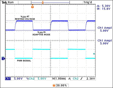
Figure 4. VLED response to a 50% PWM signal.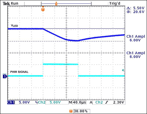
Figure 5. VLED response to a 3% PWM signal.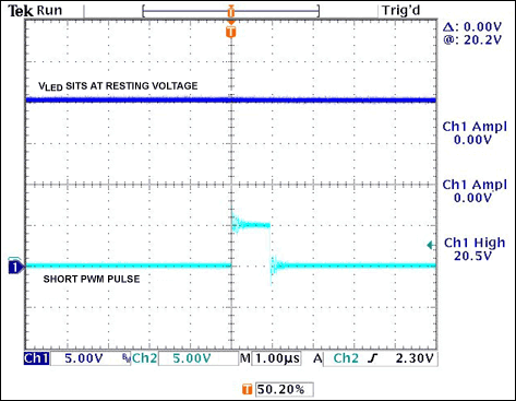
Figure 6. VLED response to a 1µs PWM signal.
Compensation
Compensation for the SEPIC is relatively simple. Current-mode control reduces the power loop to a single-order pole based on the output capacitance and load resistance. Stability requires a Type 2 compensation network. Since the load is basically static, the control loop can be relatively slow. The only real issues are the dual control loops (adaptive and resting) and the dramatically different input resistance that they present (R1 = 210kΩ, R2 = 10kΩ). R14 buffers the changes by presenting a large resistance relative to both R1 and R2. R14 and C5 (0.1?F) combine to form a dominant pole at a rather low frequency.
Sometimes there can be an output-voltage overshoot when transitioning from full to zero current. There are two reasons for this: 1) stored energy in the circuit inductances dumping into the output capacitors, and 2) a slow-responding control loop. If the inductive energy is dominating the overshoot, you must increase the output capacitance to limit its affect. If a slow control loop is the main culprit, an overvoltage clamp zener diode (D7 in this schematic) is very effective in solving the overshoot. Figure 7 illustrates the overshoot that would occur with and without D7.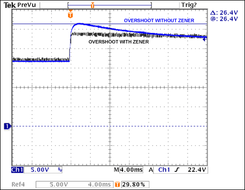
Figure 7. VLED overshoot with and without an overvoltage clamp zener diode.
Conclusion
For HB LED arrays that require wide dimming ratios, a combination of an adaptive switching regulator and linear drivers provide a sensible solution that balances the need for performance at very short on-pulses with power efficiency at larger duty cycles. SEPIC regulators are often the best switching-mode topology because of the overlapping input and output voltages that occur. With the MAX16807, you have a SEPIC controller and eight parallelable linear drivers to form the basis of your design.