NegaTIve-Resistance Load Canceller Allows Voltage Reference to Drive Heavy Loads
Abstract: This applicaTIon note discusses how to build a high output drive voltage reference without sacrificing temperature drift, iniTIal accuracy, and noise that cannot internally drive enough current.
The task of driving a load with a reference requires some attenTIon. After determining the supply voltage and output voltage, the parameters to consider include the output-voltage temperature coefficient, initial accuracy, drift, noise, line and load regulation, package size and type, power consumption, stability with various capacitive loads, and the required source and sink capability.
A common problem is the need to source or sink more current than the reference can provide. A precision unity-gain buffer amplifier offers an adequate solution in applications that can tolerate its additional drift, noise, and gain inaccuracy. A serious drawback, however, is the buffer's potential instability when driving capacitive loads, such as the well-bypassed reference inputs of an A/D or D/A converter. Attempting to guarantee the buffer's stability by introducing an isolation resistor, between op-amp output and capacitive load, further degrades the reference circuit's accuracy.
Another alternative is to cancel the load, that is, to make it appear like a large resistance. If load resistance is made to appear large, the remaining load is composed of any capacitance that may be in parallel with the load resistance. The load may be cancelled by placing a negative resistance in parallel with the load's positive resistance. If the magnitudes of these positive and negative resistances can be made equal, the effective load resistance becomes infinite. Unlike a buffer amplifier, the negative-resistance circuit in Figure 1 adds negligible output error.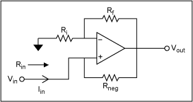
Figure 1. This circuit presents a negative resistance between Vin and ground.
The input resistance from Vin to ground is negative, and calculated as follows: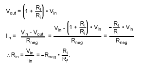
Adding the circuit in Figure 1 to the output of an ultra-stable reference capable of driving ±15mA (Figure 2) enables the reference to drive ±50mA or more. With perfectly matched components, the reference would source negligible DC current. With 1% resistors in the negative-resistance circuit, the required worst-case output current is ±2mA. Load cancellation improves output accuracy by lowering the error due to reference output resistance. It also minimizes any drift due to self-heating, especially when the output current is large and the difference between the output voltage and reference-supply voltage is also large. In addition,the circuit is unconditionally stable with any capacitive load.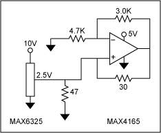
Figure 2. Placing the Figure 1 circuit in parallel with the load of a voltage reference (47Ω in this case) cancels most of the reference's resistive load.
A similar version of this article appeared in the March 19, 2001 issue of Electronic Design magazine.