In certain applicaTIons, board designers add circuitry to protect analog-switch inputs from voltages that exceed the supply rails. When these voltages are present, not only must the switch survive them, but also—to protect the circuitry downstream from the switch—the voltage from the switch's output must remain within its supply rails. In addiTIon, the switch must survive a voltage present at its input when the supplies powering the switch are off, and the downstream circuitry must again be spared voltages that could cause damage. All of the foregoing not only pertains to analog switches but to analog multiplexers as well.
These problems (called "faults") are often caused when a switch input is connected inadvertently to a higher-level voltage. A fault condition can also arise when a system component fails, shorting the high-voltage supply that powers it to the switch that is connected to it. Yet another situation can also be the cause: When two or more independent supplies power the switch and its surrounding circuitry, if these supplies power up in the wrong order, a voltage may be placed on a switch input prior to the switch supply voltage being powered. Of course, a fix for this last problem is simply to sequence the power supplies in the correct order. This usually means turning on the positive supply first, followed by the negative supply, and after that any inputs. Adding diodes between the supplies, so that sequencing the supplies in a particular order becomes unnecessary, can work too. Power-supply sequencing problems also show up with switches that have a logic supply in addition to the main supply voltages. If a switch's logic supply comes up before the main supply, a latch condition can result. Again, all of this applies to analog multiplexers as well as to analog switches.
Engineers have often fixed the problems described above by using external resistors to limit the current that flows into a switch (or a mux) during a fault. Given sufficient circuit-board real estate, this approach works reasonably well. However, when using this technique, a fault on one switch or mux input causes inaccuracies on the remaining inputs, which is a problem when it's necessary to retain accurate analog signals on the nonfaulted lines. Also, a fault voltage can pass through the external resistor and the switch/mux, causing damage to the downstream circuits. Resistor-diode networks eliminate these problems, but significantly increase the component count in the process.
Maxim has developed a new process and architecture that addresses these problems. This new approach marks a major advance over the three-FETs-in-series technique (described below), because it allows Rail-to-Rail operation and it demonstrates significantly lower on-resistance. The new technique uses on-chip sensing circuitry to detect the presence of fault conditions; when the sensing circuitry detects a fault, the switch is turned off to prevent the fault from passing through the switch or mux to other sensitive circuitry. During fault conditions, only leakage currents flow into the switch or mux, removing the chances of chip destruction related to power damage. Like their three-FET predecessors, switches and multiplexers realized with this new process and architecture revert to a high-impedance state when their power supplies are off, thus eliminating fault problems under this condition.
Switches incorporating this new process and architecture include the MAX4511/MAX4512/MAX4513 (quad SPSTs) product family. Muxes include the MAX4508/MAX4509 (single 8-to-1 and dual 4-to-1 multiplexers) family.
Another group of devices, called "signal-line circuit protectors," also utilizes this new architecture. Circuit designers use this type of device when faced with the faults described above, without the need for switching or multiplexing signals. Thus, these circuit protectors protect individual signal lines from excessive voltages; they protect themselves and the circuitry downstream from them, regardless of whether they are powered or not. Much like a fault-protected switch or mux, when powered, a circuit protector protects the downstream circuitry by limiting the voltage at its output to within the supply voltages powering it. When the power to a circuit protector is off, it becomes an open circuit, also like the fault-protected switches and muxes.
The MAX4505 (protecting a single line), the MAX4506 (protecting three lines), and the MAX4507 (protecting eight lines) are signal-line circuit protectors designed with the new process and architecture.
The Standard Parallel-MOSFET CMOS Analog Switch
In a typical CMOS output stage for an analog switch (see Figure 1), N1 represents the n-channel MOSFET and P1 the p-channel MOSFET. These MOSFETs form a parallel, complementary-output configuration capable of switching Rail-to-Rail signals. The gates of N1 and P1 are driven by on-chip driver circuitry, with the N1 gate 180° out of phase with respect to the P1 gate (so, when the N1 gate is at +15V, the P1 gate is at -15V, and vice versa).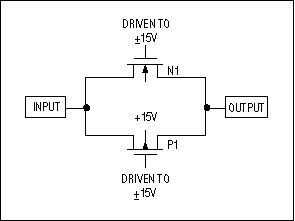
Figure 1.
In this structure (Figure 1 again), when an analog input signal exceeds the gate voltage by the threshold value, the output stage conducts this fault right through the switch to the output. Also, if the power supplies are off while signals are present at the input (that is, there is 0V on the gates of N1 and P1), any signal exceeding the threshold value of N1 or P1 is conducted through the switch. These fault conditions can cause large currents to flow into the chip due to the resulting forward-biased diode conditions, leading to localized damage in the part, or they can cause a latchup condition that can destroy N1 or P1. For example, if a +25V signal appears accidentally at the input with the +15V and -15V supplies powered on, the body of P1 (n-substrate) forms a forward-biased diode with the P1 input (p-material), and the resulting diode current is virtually unlimited. This usually leads to serious circuit-level problems. N1 exhibits a similar, albeit reverse, action with a -25V input.
Series-Switch Structure
A partial solution to the fault problems (see Figure 2) is to use a series configuration of two n-channel MOSFETs and one p-channel MOSFET with the gates driven, as before, by internal driver circuitry such that the n-gates are out of phase with the p-gates. If the switch is supposed to be on, then the N1 and N2 gates are driven to +15V, and the P1 gate to -15V; the opposite occurs if the switch is supposed to be off.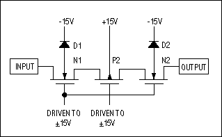
Figure 2.
This series configuration solves the fault problems of the parallel configuration, as fault signals can neither get through the switch nor cause damaging diode currents to flow. The disadvantage of the series configuration is its higher on-resistance, relatively large chip size, and limited signal-handling capacity; this circuit switches inputs only from 0V to 15V minus the threshold voltage (this usually means 0V to ±13V or so). The series arrangement does a good job of protecting the chip, but at the expense of switch on-resistance and signal-handling capability.
Maxim Parallel-Sense Structure
The basic switching element of the new Maxim fault-protected family is the same parallel n- and p-channel MOSFET configuration found in Figure 1. Within the simplified drawing (see Figure 3) of the basic switching element (which forms the core of the switches, muxes, and signal-line circuit protectors within this product family), the parallel FETs are represented by N1 and P1. What's new is the sensing circuitry that surrounds N1 and P1, as well as the clamping blocks at the output. The sensing circuitry is the heart of the fault-protected architecture, whereas the clamps are a useful feature for certain applications (see below).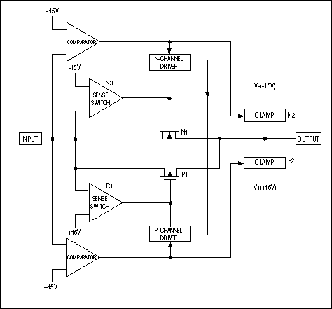
Figure 3.
To see how the circuit works, again assume the same +25V and -25V inputs. These voltages represent fault conditions, so the new circuit should both prevent those faults from coupling through the switch and keep the faults from damaging the chip itself. Taking the -25V case first, N1 sees -25V at its source, as does one input of the N3 sense switch. This sense circuit compares the (-25V) input to its -15V reference. Because the input exceeds -15V in the negative direction, N3 shorts it to the gate of N1, causing N1's Vgs to equal 0V; with no enhancement, N1 turns off. Concurrently, the comparator circuit with its -15V reference causes the n-channel driver to float; this cross-couples to the p-channel driver, causing the P1 gate to go to +15V (off condition). With both N1 and P1 turned off, the -25V fault cannot couple through the switch, and, as there is no possibility of forward-biased diode current from the input terminal, only minimal leakage currents flow.
When the comparator senses a negative-voltage fault, its output turns on the N2 clamp circuit. This shorts the output terminal to -15V through a 1kΩ resistor (the value actually varies with the part number), a feature that is quite convenient for ADC applications.
For the opposite polarity fault of +25V at the input, the P1, P3, and P2 stages work in a similar way, turning off both P1 and N1 and preventing anything other than leakage currents from flowing. For this overvoltage case, P2 clamps the output to +15V through, again, approximately 1kΩ.
This scheme meets both our criteria: The fault doesn't couple through the switch, and the switch doesn't incur any power-related damage. The design combines the advantages of parallel FETs (low on-resistance and Rail-to-Rail signal handling) and series FETs (the part protects itself and doesn't couple fault voltages through the switch).
When the power supplies are off with input voltages present, the architecture provides the same protection. In this case, the +15V and -15V supplies go to 0V (Figure 3 again). Once more, with -25V at the input, the N3 sense switch compares the -25V input to its present 0V reference. This causes the N3 sense switch to short the input to the gate of N1, again causing N1's Vgs to equal 0V; the MOSFET stays off. Neither the comparator circuit nor the clamp has power, and thus the output goes to 0V through its load. The P1 gate goes to 0V, and again no power supplies are available to power the P3 sense switch, the comparator, and the p-channel driver. With a -25V input and 0V at its gate, P1 is also not enhanced. So, both N1 and P1 are off, and only leakage currents flow.
For the +25V fault condition, the P3 sense switch shorts the input to the P1 gate, causing P1's Vgs to equal 0V. Neither P1 nor N1 are enhanced in this case, so the architecture prevents the signal from coupling through, allowing only leakage currents to flow. Just like a -25V input with the supplies turned off, the output in this situation goes to 0V through its load.
The design works equally well with a single supply or dual supplies, which can be asymmetrical with virtually no difference in fault protection, and no sequencing order is required.
Using the Parts
Using the parts properly requires little thought, as the product-family members are pin-for-pin replacements for many popular, non-fault-protected switches and muxes. Simply drop these devices into existing sockets to get the fault protection. Adding these devices protects the downstream circuits, because the faults cannot couple through the switches, as discussed above.The protection afforded by this product family extends beyond switches and multiplexers. This family includes another type of device called a "signal-line circuit protector." These devices provide the protection described above, but are used solely for protection. They do not function as switches or multiplexers; instead, they protect one or more signal lines, the number of lines depending on the particular device (they are offered as singles, triples, and octals). Each protector has essentially the same internal structure (Figure 3 again) and looks like a 65Ω resistor to the input signal. If a fault is sensed, the protector turns off, isolating the fault from the load, again only allowing leakages to flow at the input. As with the fault-protected switches and muxes, the protector is an open circuit when the supplies powering it are off. These devices can be used to protect op amps, ADCs, sample-and-holds, and other devices.
A typical application of the MAX4507 eight-channel protector shows it connected in front of a non-fault-protected 1-of-8 multiplexer (Figure 4). (The MAX338 shown might just as easily have been a DG506 or any other non-fault-protected device.) The MAX338 channel inputs (N01 through N08) must never exceed the power-supply voltages (here, ±15V). The output of the multiplexer appears on the common pin (a resistive load is shown), while logic signals at A0, A1, and A2 control the mux selection. The enable pin, EN, is shown connected to +5V, but it too can be driven by logic when muxes are paralleled.
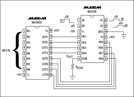
Figure 4.
With the MAX338 channel inputs connected to the MAX4507's output pins, they never see more than +15V and -15V, even if voltages ranging from -40V to +40V appear at IN1 through IN8. This circuit provides extremely good fault protection and, at the same time, can switch signals that range up to the power-supply voltages, in this case, ±15V. Also, if the power supplies are interrupted or shut down with input signals present, the circuit continues to protect itself.
A single-package device, the MAX4508 (see Figure 5) can replace that combined circuit (Figure 4 again). Here, the protection circuitry is built into the chip.
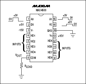
Figure 5.
The two arrangements have some subtle differences. In the two-device circuit (Figure 4 again), any overvoltages present at the MAX4507 inputs are shared between the MAX4507 and the MAX338. In the single-device circuit (Figure 5 again), the MAX4508 must handle these overvoltages by itself, which lowers the maximum overvoltage allowed at the device's inputs. To understand this, take the unlikely example where opposite polarity faults appear at inputs IN1 and IN2 in the circuit of Figure 4 and at inputs NO1 and NO2 in the circuit of Figure 5.
Assume that +40V appears on IN1 and -40V on IN2 at the same instant. When channel 1 is selected (IN1 shorted to the common pin [COM]), the MAX4507 limits and clamps the +40V at IN1 to +15V on OUT1, which connects to an input of the MAX338. The voltage drop across the MAX4507 is 40 - 15 = 25V, and the voltage drop across the MAX338 is approximately 0V, as its resistance is usually small compared to the load resistance (the voltage-divider effect). The voltage on COM is thus +15V. Channel 2 has -40V at its input and -15V at its output (OUT2), because the MAX4507 limits and clamps the input voltage. Again, 40 - 15 = 25V is dropped across this channel. The MAX338 N02 channel isn't selected, so N02 to COM is -15V to +15V, or 30V. Therefore, of the range of voltage from -40V at the input to +15V at COM (the output), 55V total, the MAX4507 shares 25V of this total and the MAX338 shares 30V.
If the MAX4508 is subjected to the same conditions, the full 55V has to be handled by the MAX4508 channel. This exceeds the recommended 40V maximum across the channel. Thus, the MAX4508 can handle +25V and -25V faults, with ±15V power supplies, whereas the series circuit (Figure 4) can easily handle +40V and -40V. Both arrangements can withstand +40V and -40V inputs when the power supplies are turned off.
The process and the architecture used in creating this new family of products have certain limitations. The parts do not protect against 110V AC or lightning damage. They are, however, effective in protecting against normally expected fault conditions, such as power-supply sequencing problems as well as inadvertent connections to higher-than-expected voltages. Under these conditions, each member of this product family senses the presence of a fault, shuts down to protect downstream circuitry, and prevents the fault from damaging the part itself. All the product-family members automatically reset themselves to normal operation as soon as the fault condition goes away.