An input fault condition occurs when a voltage applied to the input of a switch, mux, or signal-line circuit protector exceeds the voltage at the power supply pins. Discrete components can be used to protect against these faults, but fault-protected switches, multiplexers, and signal-line circuit protectors offer a more practical approach.
Faults can occur when:
- A signal applied to an external connector that routes to an input of a switch, mux, or circuit protector is too high.
- The power is turned off and the supply voltage falls to zero (at which point any non-zero voltage applied to an input is a fault.)
- A sensor or other device fails, shorting the high-voltage supply that powers the device to the device's output, which connects to a switch, multiplexer, or circuit protector.
- Multiple supplies providing power do not follow the proper power-up and power-down sequencing.
Fault Protection for Multiplexers
An aircraft hydraulic system provides an example of fault voltages that result from component failure (Figure 1). In this case, a computerized alarm generator and a cockpit display scan multiple pressure sensors. When a transducer fails and shorts the full aircraft-battery voltage of 28V to its output, damage happens not only to the multiplexers, but also to the downstream alarm and cockpit-display circuitry. Under this fault condition, aircraft engineers, of course, want to avoid component damage, regardless of whether the multiplexers have power. But they also want to ensure that pilots can continue to accurately read the measured pressure and hear the alarms that the working pressure transducers generate. Further, in the event that the alarm or the cockpit-display circuitry loses power, the circuitry that still has power must continue to properly read the hydraulic pressure. Aircraft engineers impose this latter condition to not only improve flight safety, but also to allow accurate readings during maintenance-when power to any component can be on or off at random.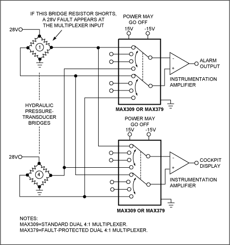
Figure 1. An aircraft hydraulic system illustrates the need for fault protection. A short circuit through a pressure sensor can cause 28V to come into direct contact with the multiplexers.
When the circuit or system subjects a standard multiplexer to this 28V fault voltage, the multiplexer not only incurs damage, it also passes the high voltage to the nonfaulted side of the multiplexer. Also, when a fault appears at an off channel, current injects into the substrate of the multiplexer, rendering the on channel inaccurate. Finally, when you remove power to one of the multiplexers, the multiplexer loads the signals from the sensors.
To deal with some or all of these problems, several fault-protection schemes have emerged over the years. A common remedy is to add resistors in series with the multiplexer inputs (Figure 2). This scheme limits to safe levels the current that flows into the multiplexer's input-protection diodes when a fault occurs. Typically, two protection diodes are present at each input: one connects from the input to the positive supply, the other from the input to the negative supply. These diodes prevent voltages at the input from ranging beyond a diode drop above the positive supply and beyond a diode drop below the negative supply. These diodes protect against ESD voltages and voltages that originate from relatively high-impedance sources. The diodes do not protect against constant fault voltages from low-impedance sources unless you add a series resistor. The specified maximum allowable continuous current for a particular multiplexer pin is actually a rating of the current-handling capability of the protection diodes connected to that input. You will find this number in the Absolute Maximum Ratings of the multiplexer data sheet.
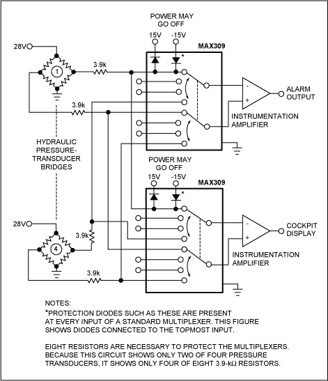
Figure 2. Adding resistors between the pressure sensors and the multiplexers provides fault protection but allows inaccuracies in the nonfaulted multiplexer channels.
For the circuit of Figure 2, the worst-case current through the protection diodes occurs when the power to the multiplexer is off (at 0V) and when the 28V supply reaches its upper tolerance of approximately 36V. Under these conditions, the 3.9kΩ resistors limit the current to less than 10mA. Actually, the current through the protection diodes is closer to half this amount, because two protection diodes parallel each other in this situation. For each of the inputs that you tie together, the diode that connects to the positive rail at one input parallels the diode that connects to the positive rail at the other input. Because data sheets do not divulge much about the characteristics of protection diodes, you can assume that these diodes are so poorly matched that one diode steals all the current from the other. Thus, this circuit uses 3.9kΩ resistors, which limit the current to less than 10mA with a 36V fault when the positive supply is 0V (and assuming one of the two paralleled diodes takes all the current).
This scheme also protects the downstream circuitry, because the resistors prevent damage to the multiplexer's input-protection diodes, which thus continue to limit the voltage to the downstream circuitry to a diode drop outside the supply rails. However, this protection scheme can not protect against certain errors when a fault isn't present. If power is off at one multiplexer, its protection diodes will usually connect to 0V via the off supplies. The protection diodes within that multiplexer that connect to the positive supply, which is now at 0V, will conduct enough current through the 3.9kΩ resistor to cause an error of several volts. To fix this problem, you can double the number of protection resistors by connecting one resistor to each multiplexer input.
Series Resistors Have a Downside
These protection resistors, unfortunately, add to the effective source resistance, which, in concert with the multiplexer's input leakage, increases the error voltage. Also, if a fault occurs in an off channel, current flows through the multiplexer's substrate, which generates error currents in the on channel. These error currents reduce the accuracy of the measurement. Adding these resistors increases the circuit's size and impedance level, which makes it more susceptible to noise pickup.Two other problems can affect circuit performance when you add these resistors, although not for this particular application. First, the circuit loses some bandwidth, but usually not enough to hamper most applications. The aircraft-hydraulic application, for example, operates at DC. Assuming about 3pF of input capacitance and a 3.9kΩ resistor at each input-unlike in Figure 2, for which two channels share a resistor-each channel's bandwidth decreases to about 13MHz. Second, these resistors create inaccuracies due to voltage-divider losses. In this application, however, the high input impedance of the instrumentation amplifier prevents any appreciable voltage-divider effects from occurring.
When a number of 28V fault voltages simultaneously appear at the multiplexer inputs, the current that flows through the internal protection diodes that connect to 15V can drive up this supply voltage. Similarly, negative fault voltages can drive the -15V supply more negative. The circuit in Figure 3 protects against both this problem and the problem of substrate current flow. In this circuit, resistor/diode networks clamp the multiplexer inputs below the supply voltages, limiting the voltage at the multiplexer inputs and eliminating current flow through the multiplexer's protection diodes. When power to the multiplexer is on, a fault to the circuit does not send current into the substrate. Thus, off-channel faults do not affect the channels that are on. Also, because no current flows through the protection diodes, fault voltages can not affect the supply voltages via that path.
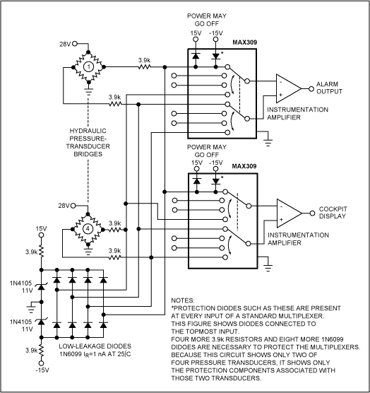
Figure 3. Protection circuitry prevents the protection diodes within the multiplexers from turning on during faults, which eliminates the errors that would otherwise occur in the nonfaulted channels.
The circuit uses low-leakage silicon diodes for the clamps. You should avoid using Schottky diodes because their leakage currents create an appreciable voltage drop across the 3.9kΩ resistors. Using low-leakage silicon diodes alone will not do the trick, however. When these diodes connect directly to the ±15V supplies, their forward voltage drops of approximately 0.65V allow a fault voltage to exceed the absolute maximum rating of the multiplexer inputs, which is usually 0.3V above the rails. Thus, the circuit uses two 1N4105 Zener diodes to drop the supply voltages for the silicon diodes to ±11V.
Note that two 3.9kV resistors bias the Zener diodes. It might be tempting to leave the Zeners unbiased, instead relying on fault voltages to bias them when a fault occurs. However, leaving these diodes unbiased will create problems, because a Zener that isn't reverse-biased draws leakage current below the threshold. If that leakage current flows through the circuit, this current would create an error that varies with temperature and the Zener's applied voltage-an ugly problem.
The major problem with this clamp technique is the number of components: Ten 3.9k resistors, sixteen 1N6099 diodes, and two 1N4105 diodes. Board space, cost, and reliability concerns arise with the addition of so many parts. Also, removing power from one multiplexer loads the other multiplexer. You have to add an additional resistor at each multiplexer input to prevent this problem. Further, as with the circuit in Figure 2, the 3.9k resistors add to the impedance of the signal path, which increases the chance of noise problems. Finally, in certain applications, problems can occur due to bandwidth limitations and voltage-divider effects.
Switches and Multiplexers with Internal Fault Protection
Maxim produces a line of switches that incorporates fault-protection circuitry. Fault protection not only protects the switch from inadvertent overvoltages, but protects any downstream circuitry as well. When a fault condition is detected, these switches use comparators to turn off the gate driver to the pass transistors, thereby stopping the flow of anything other than leakage currents.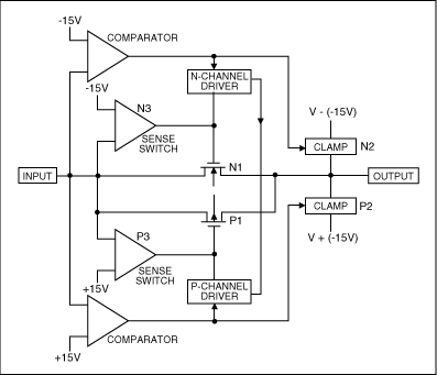
Figure 4. A fault-protection switch uses comparators to turn off the gate driver to the pass transistors.
To see how the circuit works (Figure 4), assume the same +25V and -25V inputs as discussed above. These voltages represent fault conditions. The new circuit should, therefore, both prevent those faults from coupling through the switch, and keep the faults from damaging the chip itself.
We shall examine the -25V case first. N1 sees -25V at its source, as does one input of the N3 sense switch. This sense circuit compares the -25V input to its -15V reference. Because the input exceeds -15V in the negative direction, N3 shorts it to the gate of N1, causing N1's VGS to equal 0V. N1 turns off. Concurrently, the comparator circuit with its -15V reference causes the n-channel driver to float; this cross-couples to the p-channel driver, causing the P1 gate to go to +15V (off condition). With both N1 and P1 turned off, the -25V fault cannot couple through the switch and, as there is no possibility of forward-biased diode current from the input terminal, only minimal leakage currents flow.
When, furthermore, the comparator senses a negative-voltage fault, its output turns on the N2 clamp circuit. This shorts the output terminal to -15V through a 1kΩ resistor, a feature that is quite convenient for ADC applications. (The resistor value actually varies with the part number.)
Turning now to the opposite polarity fault of +25V at the input, the P1, P3, and P2 stages work in a similar way: turn off both P1 and N1 and prevent everything except leakage currents from flowing. For this overvoltage case, P2 clamps the output to +15V through, again, resistor of approximately 1k . This scheme meets both desired criteria. First, the fault does not couple through the switch, and, secondly, the switch does not incur any power-related damage. This design combines the advantages of parallel FETs (low on-resistance and rail-to-rail signal handling) and series FETs (the part protects itself and does not couple fault voltages through the switch).
When the power supplies are off with input voltages present, the architecture in Figure 5 provides the same fault protection. In this case, the +15V and -15V supplies go to 0V.
Once more, with -25V at the input, the N3 sense switch compares the -25V input to its present 0V reference. This causes the N3 sense switch to short the input to the gate of N1, again causing N1's VGS to equal 0V. The MOSFET stays off. Neither the comparator circuit nor the clamp has power, and thus the output goes to 0V through its load. The P1 gate goes to 0V, and again no power supplies are available to power the P3 sense switch, the comparator, and the p-channel driver. With a -25V input and 0V at its gate, P1 is also not enhanced. As a result, both N1 and P1 are off, and only leakage currents flow.
For the +25V fault condition, the P3 sense switch shorts the input to the P1 gate, causing P1's VGS to equal 0V. As neither P1 nor N1 are enhanced in this case, the architecture thus prevents the signal from coupling through; the design allows only leakage currents to flow. As with a -25V input with the supplies turned off, the output in this situation goes to 0V through its load.
The design works equally well with a single supply or dual supplies, which can be asymmetrical with virtually no difference in fault protection. No sequencing order is required.
Maxim switches are usually fault protected to ±40V. That means that with a ±15V supply the device has a ±25V of fault protection headroom. The MAX4505, MAX4711, MAX4712, MAX4713, MAX4510, and MAX4520 are some examples of a fault-protected switch.
Fault-Protected Multiplexers Reduce External Components
An alternative to adding protection components to a standard multiplexer is to use a fault-protected multiplexer. A fault-protected multiplexer operates like a standard multiplexer, except that it protects against fault voltages without the addition of external components. When the circuit subjects any of the inputs of such devices to a fault, the input goes into a high-impedance state, limiting the current the inputs can draw. The inputs also limit the voltage appearing at the multiplexer's output during a fault, which prevents damage to downstream circuitry. Unlike standard multiplexers, these devices guarantee a high-impedance path from all inputs to the output when you remove the power. Thus, a fault that occurs when the multiplexer is not powered cannot damage the multiplexer or harm the downstream circuitry.You could, for example, substitute two MAX379 differential four-channel fault-protected multiplexers in the circuit of Figure 1, allowing protection against ±75V faults when power to the multiplexer is off. When the ±15V supplies are on, the multiplexer can withstand ±60V fault voltages.
The major advantages to using a fault-protected multiplexer are:
- All channels turn off when you remove power.
- Only nanoamperes of current flow during any fault condition.
- During faults, output-signal limits are 3V less than the supply voltages. Thus, high voltages cannot get through the multiplexer to damage downstream circuits.
- Newer fault-protected multiplexers allow the output signals to range up to the supply voltages.
- No series protection resistors or clamp diodes are necessary.
- The device protects both as a multiplexer and a demultiplexer.
- Off-channel faults do not affect on-channel accuracy.
Fault Protection for Switches
When two or more supplies power a system, sequencing them in the wrong order can cause fault voltages to appear at multiplexer and switch inputs, as well as other components. In Figure 5, a sensor assembly connects to another assembly that includes an SPDT switch and an ADC. If, for example, the 15V and -15V supplies come up at different times, the op amp's output saturates at the rail that comes up first, and a fault occurs even if ±5V power is present at the SPDT switch. A fault condition also exists at the switch if the ±15V supplies power up simultaneously when the ±5V supplies are off.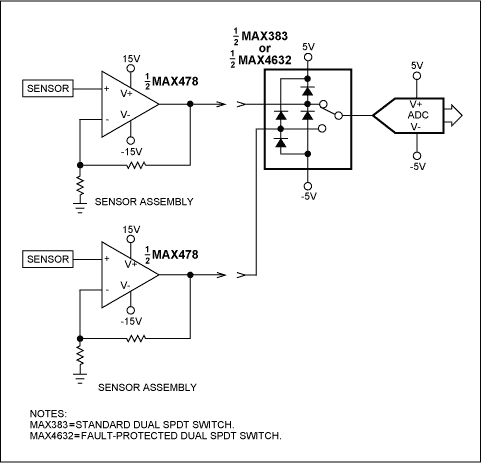
Figure 5. When several supplies power two assemblies, power-supply sequencing problems can cause fault voltages.
The techniques for protecting the multiplexer circuit apply equally well to switches. Just as with a multiplexer, placing resistors in series with the switch inputs protects against damage to the switch during a fault. However, these resistors cause inaccuracies in the other switches within the same package that do not have a fault condition. When a fault voltage turns on a protection diode, current flows into the substrate, which causes inaccuracies in the nonfaulted switches. Also, these resistors cause additional errors due to leakage currents and voltage-divider effects.
You must take care to ensure that the circuitry downstream from the specific switch undergoing a fault can handle the current that flows through the switch under this fault condition. For the circuit of Figure 5, this current is not an issue because of the relatively high input impedance of the ADC. In circuits for which the switch drives a device with low input impedance, the current during a fault can be quite high. The voltage at the switch is a diode drop above the supply voltage, and the on-resistance of the switch essentially determines the current that this voltage creates. However, when an op amp drives a protection resistor and switch, the current during a fault usually can not cause damage, because the output-current capability of most op amps is relatively limited. In fact, even without a protection resistor, the protection diodes within the switch should, in most cases, limit the voltage from the op amp to a diode drop outside the supply voltages that power the switch. Under these conditions, however, if the op amp were housed in an SC-70 package, power dissipation could become a consideration. Most of these same concerns about excessive current apply to the multiplexer circuits if the multiplexer drives a low-impedance device instead of an instrumentation amplifier.
Regardless of whether you use a protection resistor, a fault does cause inaccuracies in the nonfaulted switches. You can use the protection scheme in Figure 3 to prevent fault voltages from generating these errors. Here again, the number of components required may be prohibitive, with cost, reliability, and board real estate becoming an issue. Also, if a current-limiting resistor is necessary-for example, if the op amp's output can source a large amount of current-two more problems arise. First, the resistor may make the time to charge the ADC's sample capacitor prohibitively long. Conversion errors result if the ADC samples the voltage before the sample capacitor has fully charged. Second, ADCs prefer low-impedance sources because current spikes drawn by the ADC input can cause voltage errors at that same input. The resistance of the current-limiting resistor plus the switch on-resistance may be sufficiently high to cause this problem.
The simplest approach is to incorporate into the circuit a fault-protected SPDT switch, such as the MAX4632. In this situation, this switch is suitable because the fault voltage does not exceed ±35V, which is the switch's permitted level with a supply voltage of ±5V.
The major advantages to using a fault-protected switch follow:
- All switches turn off when you remove power.
- Only nanoamperes of current flow during any fault condition.
- During faults, output signals do not exceed the supply voltages. Thus, high voltages cannot get through the switch to damage output circuits, yet these switches allow signals that range up to either voltage rail to pass through. The first generations of these switches allow a somewhat smaller range of signals to pass, however.
- No series protection resistors or clamp diodes are necessary.
- Faults on any other switch within the same IC do not affect the accuracy of nonfaulted switches.
All first-generation fault-protected switches, multiplexers, and circuit protectors are free of latch-up problems. You can sequence their supplies in any order without causing a latch-up condition, regardless of whether voltages are present on any of the devices' pins. In fact, some engineers use fault-protected switches and multiplexers, not to protect against faults, but simply to avoid latch-up problems. Second-generation devices, however, cannot tolerate fault voltages on their output pins, because those pins have internal clamps to the rails. This feature is typically not a problem, because most applications require fault protection only on the input side. Also, if a voltage is present on a control pin when these multiplexers' supplies are off, the multiplexer can pass an input voltage to the output. The magnitude of the output voltage equals the voltage on the control pin minus a diode drop. Further, both the first- and second-generation devices temporarily pass fault voltages during power up when using bipolar supplies that do not simultaneously power up. Fortunately, under those conditions, these devices limit the voltage that passes to the output to less than the supply voltage at either rail. In other words, a positive fault voltage cannot exceed the voltage at the positive supply, and a negative fault voltage cannot exceed the voltage at the negative supply. Third-generation devices will soon be available that will allow faults on all pins and prevent the passing of fault voltages when bipolar supplies do not simultaneously power up.
Fault Protection Without Switching
Figure 6 shows the same circuit as Figure 5 but for a situation that does not require switching. Protection is necessary only if the op amp can source enough current to damage the ADC's protection diodes. It may be tempting to use only a resistor to limit the current into the ADC's protection diodes, because a resistor can limit the current into the ADC sufficiently to prevent damage to the diodes. However, the addition of the resistor will likely increase the time to charge the ADC's sample capacitor too much, resulting in erroneous readings.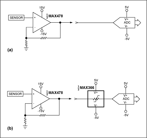
Figure 6. Sequencing problems cause fault voltages in circuits without switches and multiplexers (a). A signal-line circuit protector provides optimal protection against faults that appear on individual lines rather than at switches and multiplexers (b).
A signal-line circuit protector provides the required protection in this situation (Figure 6b). Signal-line circuit protectors are also useful when the inputs of an integrated multiplexer/ADC require fault protection. This device protects a single circuit path; it provides the same type of protection as a fault-protected switch or multiplexer but does not switch signals. The MAX366 in Figure 6b comes with three circuit protectors. With ±5V supplies, the MAX366's on-resistance is typically 85Ω when the input voltage to the device is 0V. Take care when using this device, however, because its on-resistance rises as the input voltage varies from zero, particularly in the negative direction. With an approximately -2V input, the on-resistance rises to 150Ω, whereas an input of about 2.4V results in that same resistance. The MAX4506, which is pin-compatible with the MAX366, demonstrates a much flatter on-resistance, but requires a higher bipolar supply voltage than this application provides.
A similar version of this article appeared in the May 2, 2002 issue of EDN magazine.