|
|
Introduction
First developed about 25 years ago, integrated analog switches often form the interface between analog signals and a digital controller. This tutorial presents the theoretical basis for analog switches and describes some common applications for them. The special features of calibration multiplexers (cal-muxes), fault-protected switches, and force-sense switches are discussed as well.In recent years, integrated analog switches have offered better switching characteristics, lower supply voltages, and smaller packages. Because so many performance options and special functions are available, the well-informed product designer can usually find the right part for a particular application.
Standard Analog Switches
CMOS analog switches are easy to use, so most designers take them for granted. But one should not forget that these switches solve specific engineering problems. Conventional analog switches like the early CD4066 or the MAX4066 are now offered by many semiconductor manufacturers; their structure is shown in Figure 1. Maxim also offers devices such as the MAX4610, which is pin-for-pin compatible with the industry standard but offers better performance.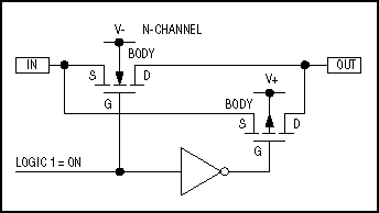
Figure 1. The internal construction of a typical analog switch features parallel n- and p-channel MOSFETs.
Connecting an n-channel MOSFET in parallel with a p-channel MOSFET allows signals to pass in either direction with equal ease. Whether the n- or the p-channel device carries more signal current depends on the ratio of input to output voltage. Because the switch has no preferred direction for current flow, it has no preferred input or output. The two MOSFETs are switched on and off by internal inverting and noninverting amplifiers. These amplifiers level-shift the digital input signal as required, according to whether the signal is CMOS- or TTL-logic-compatible and whether the analog supply voltage is single or dual.
Low-Resistance Switches
Taking the p- and n-channel on-resistances (RON) in parallel (product over sum) for each level of VIN yields a composite on-resistance characteristic for the parallel structure (Figure 2). This plot of RON versus VIN can be described as linear if you exclude the effects of temperature, power-supply voltage, and RON variation with analog input voltage. You should be aware that these effects represent disadvantages and that minimizing them is often the primary purpose of new products. See Table 1.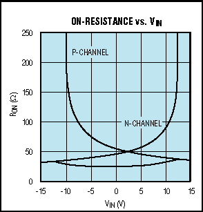
Figure 2. The n-channel and p-channel on-resistances of Figure 1 form a low-valued composite on-resistance.
Table 1. Low-Resistance Switches
| Part Number | Function | RDS(ON) (Ω max) |
ICOM(OFF)/ ID(OFF) (nA max) | RON Match (Ω max) |
RON Flatness (Ω max |
tON/tOFF (ns max) | Charge Injection (pC typ) | Supply Voltage Range (V) | Pin- Package |
| MAX312/3/4 | 4 SPST NC/ NO/ NO,NC | 10 | 0.5 | 1.5 | 2 | 225/185 | 30 | ±4.5 to ±20 | 16-DIP|SO |
| MAX4614/5/6 | 4 SPST NO/ NC/ NO,NC | 10 | 1 | 1 | 1 | 12/10 | 6.5 | +2 to +5.5 | 14-DIP/SO/16-QSOP |
| MAX4617 | 8X1 Mux | 10 | 1 | 1 | 1 | 15/10 | 3 | +2 to +5.5 | 16-DIP/SO/QSOP |
| MAX4618 | Dual 4X1 Mux | 10 | 1 | 1 | - | 15/10 | 3 | +2 to +5.5 | 16-DIP/SO|QSOP |
| MAX4619 | 3 SPDT | 10 | 1 | 1 | - | 15/10 | 3 | +2 to +5.5 | 16-DIP|SO|6/QSOP |
| MAX4621 | 2 SPST NO | 5 | 0.5 | 0.5 | 0.5 | 250/200 | 80 | ±4.5 to ±20 or +4.5 to +36 | 16-DIP/SO |
| MAX4622 | 2 SPDT | 5 | 0.5 | 0.5 | 0.5 | 250/200 | 80 | ±4.5 to ±20 or +4.5 to +36 | 16-DIP/SO |
| MAX4623 | 2 DPST | 5 | 0.5 | 0.5 | 0.5 | 250/200 | 80 | ±4.5 to ±20 or +4.5 to +36 | 16-DIP/SO |
| MAX4661/2/3 | 4 SPST NO/ NC/ NO,NC | 2.5 | 0.5 | - | 0.4 | 250/200 | 120 | ±4.5 to ±20 or +4.5 to +36 | 16-DIP/SO|/SSOP |
| MAX4664/5/6 | 4 SPST NO/ NC/ NO,NC | 4 | 0.5 | 0.5 | 0.5 | 300/200 | 300 | ±4.5 to ±20 or +4.5 to +36 | 16-DIP|/SO |
| MAX4667/8/9 | 2 SPST NO/ NC/ NO,NC | 2.5 | 0.5 | 0.4 | 0.4 | 300/200 | 450 | ±4.5 to ±20 or +4.5 to +36 | 16-DIP/SO |
| MAX4680/90/94 | 2 SPST NO | 1.25 | 0.5 | 0.25 | 0.3 | 275/200 | -60 | ±4.5 to ±20 or +4.5 to +36 | 16-DIP/WID SO/SSOP |
| MAX4734 | 1 4:1 MUX | 0.8 | 1 | 0.2 | 0.1 | 25/20 | 60 | +1.6 to +3.6 | 10-µMax 12-TQFN |
| MAX4741 | 2 SPST | 0.8 | 1 | 0.08 | 0.18 | 24/16 | 28 | 1.6 to +3.6 | 8-SOT23 |
| MAX4751 | 4 SPST NO | 0.9 | 2.5 | 0.12 | 0.1 | 30/25 | 21 | +1.6 to +3.6 | 14-TSSOP 16-QFN |
| MAX4756 | 4 SPDT NO/NC | 0.85 | 3 | 0.35 | 0.4 | 150/40 | 50 | +1.8 to +5.5 | 36-UCSP 36-TQFN |
| MAX4780 | 4 2:1 MUX | 1 | 1 | 0.15 | 0.2 | 25/10 | 5 | +1.6 to +4.2 | 16-TQFN 16-TSSOP |
| MAX4781 | 1 8:1 MUX | 1 | 2 | 0.4 | 0.2 | 25/15 | 40 | +1.6 to +3.6 | 16-QFN 16-TSSOP |
| MAX4855 | 2 SPST NO/NC | 1 | 2 | 0.12 | 0.27 | 60/40 | 170 | +2 to +5.5 | 16-TQFN 16-TSSOP |
The first analog switches operated on ±20V supply voltages and had several hundred ohms of RON. Recent products (the MAX4601, for example) achieveΩ maximum RON with a much lower supply voltage. Supply voltage has a substantial effect on RON (Figure 3). The MAX4601 specifies signal and supply voltages from 4.5V to 36V or from ± 4.5V to ± 20V. As you can see, RON increases for lower supply voltages. The max RON is about 8Ω at 5V, 3Ω at 12V, and only 2.5Ω at 24V. Many new analog switches specify low-voltage operation for supply voltages down to 2V. For 5V supplies, Figure 4 compares the Maxim switches with older types.
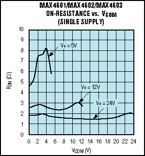
Figure 3. Higher supply voltage causes lower on-resistance.
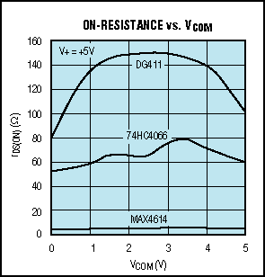
Figure 4. At +5V supply voltage, later-generation analog switches have lower on-resistance.
When selecting switches for single-supply systems, try to choose from those intended for single-supply use. Such devices save one pin, because they do not require separate V- and ground pins. As a result, this economy of pins enables a single-pole/double-throw (SPDT) switch to fit into a miniscule 6-pin SOT23 package. Similarly, low-voltage dual-supply applications call for dual-supply switches. These switches require a V- pin in addition to the ground pin, and typically specify a logic interface with standard CMOS and TTL levels. The SPST MAX4529, for example, is also available in a 6-pin SOT23 package.
Many high-performance analog systems still rely on higher-level bipolar supplies such as ±15V or ±12V. The interface to these voltages requires an additional supply pin commonly labeled VL (shown in the MAX318 data sheet). The VL supply connects to the system logic voltage, which is usually 5V or 3.3V. Having the input logic signals referenced to the actual logic levels increases the noise margin and prevents excessive power dissipation.
Often misunderstood is the analog-switch concept pertaining to input logic levels and their effect on supply current. If the logic inputs are at ground or VCC (or VL when available), analog switches have essentially no supply current. Applying TTL levels to a 5V switch, however, can cause the supply current to increase more than 1000 times. To avoid unnecessary power consumption, you should avoid TTL levels, which are simply a legacy of the 1980s.
Signal Handling
Figure 3 also shows the value of RON versus signal voltage. These curves fall within the specified range of supply voltage, because analog switches can only handle analog-signal levels between the supply voltages. Under- or overvoltage inputs can permanently damage an protected switch by producing uncontrolled currents through internal diode networks. Normally, these diodes protect the switch against short-duration electrostatic discharge (ESD) as high as ±2kV.RON for a typical CMOS analog switch causes a linear reduction of signal voltage that is proportional to current passing through the switch. This might not be a disadvantage for modest levels of current or if the design accounts for RON effects. However, if you accept a certain level of RON, then channel matching and RON flatness can interest you. Channel matching describes the variation of RON for the channels of one device; RON flatness describes the variation of RON versus signal range for a single channel. Typical values for these parameters are 2Ω to 5Ω, and only 0.5Ω maximum for very low RON switches (MAX4601, for instance). The smaller the ratio of matching/RON or flatness/RON is, the more accurate the switch.
In most applications, you can avoid excessive switch current by modifying the circuit design. To change the gain of an op amp by switching between different feedback resistances, for example, choose a configuration that places the switch in series with a high-impedance input (Figure 5a). Because switch currents are insignificant, you can ignore the value of RON and its temperature coefficient. Switch current in the alternative design (Figure 5b) can be substantial, because it depends on the output voltage.
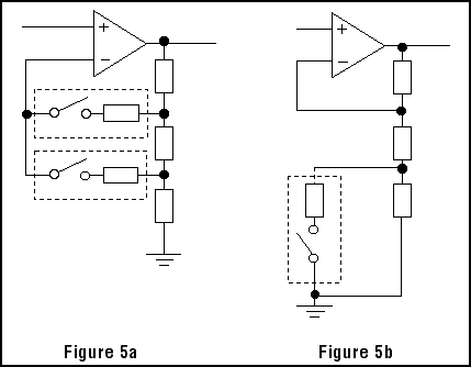
Figure 5. Gain-control circuits are good (a) or bad (b) depending on the amount of current through the switch.
Break-Before-Make
Turn-on and turn-off times (tON and tOFF) for most analog switches vary from below 60ns to as high as 1µs. For Maxim's "clickless" audio switches, tON and tOFF are in the millisecond range to eliminate the audible clicks otherwise present when switching audio signals. The relative magnitudes are also important: tON > tOFF yields break-before-make action, and tOFF > tON yields make-before-break. This distinction is critical for some applications.Figure 5a shows that you must take care in switching between the two gains. One switch is normally closed in a typical make-before-break application. In changing gain you must avoid opening both switches at once; that is, the second switch must close before the first switch opens. Otherwise, the op amp applies open-loop gain and drives its output to the rails. The opposite configuration (break-before-make) is also useful in switching among different input signals to a single op amp. To avoid short circuits between the input channels, a given connection must be switched off before the next one is switched on.
When a changing signal level modulates the on-resistance, causing a variation in the insertion loss, analog switches generate total harmonic distortion (THD). Consider a 100Ω switch with 10Ω RON flatness, for example. Loading this switch with a 600Ω termination produces 0.24% of THD. Consequently, for low THD you should avoid loading the output of an analog switch.
Charge-Injection Effects
As mentioned above, low RON is not necessary in all applications. Lower RON requires greater chip area. The result is a greater input capacitance whose charge and discharge currents dissipate more power in every switching cycle. Based on the time constant t = RC, this charging time depends on load resistance (R) and capacitance (C). It normally lasts a few tens of nanoseconds, but low-RON switches have longer-duration on and off periods. High-RON switches are faster.Maxim offers both types of switches, each with the same pinout in the same miniature SOT23 package. The MAX4501 and the MAX4502 specify higher on-resistance but shorter on/off times. The MAX4514 and the MAX4515 have lower on-resistance but longer switching times. Another negative consequence of low on-resistance can be the higher charge injection caused by higher levels of capacitive gate current. A certain amount of charge is added to or subtracted from the analog channel with every on or off transition of the switch (Figure 6). For switches connected to high-impedance outputs, this action can cause significant changes in the expected output signal. A small parasitic capacitor (CL) with no other load adds a variation of ΔVOUT, so charge injection can be calculated as Q = ΔVOUTCL.
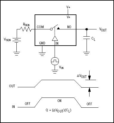
Figure 6. Charge injection from the switch-control signal causes a voltage error at the analog output.
A track/hold amplifier, which maintains a constant analog output during conversion by an A/D converter, offers a good example of this (Figure 7). Closing S1 charges the small buffer capacitor (C) to the input voltage (VS). The value of C is only a few picofarads, and VS remains stored on C when S1 opens. The held voltage (VH) is applied to the buffer by closing S2 at the beginning of a conversion. The high-impedance buffer then maintains VH constant over the ADC's conversion time. For short acquisition times, the track/hold's capacitor must be small and S1's on-resistance must be low. On the other hand, charge injection can cause VH to change by ±ΔVOUT (a few millivolts), thereby affecting the accuracy of the following ADC.
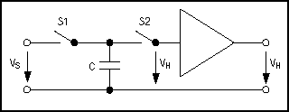
Figure 7. A typical track/hold function requires precise control of the analog switches.
Having reviewed these fundamentals, we now focus on innovative switches for special applications.
T-Switches for Higher Frequencies
The T-switch is suitable for video and other frequencies above 10MHz. It consists of two analog switches in series, with a third switch connected between ground and their joining node. This arrangement provides higher off-isolation than a single switch. The capacitive crosstalk for a T-switch turned off typically rises with frequency due to the parasitic capacitances in parallel with each of the series switches (Figure 8). The problem in operating a high-frequency switch does not lie in turning it on, but in turning it off.When the T-switch is turned on, S1 and S3 are closed and S2 is open. In the off state, S1 and S3 are open and S2 is closed. In that case (the off state) the signal tries to couple through the off-capacitance of the series MOSFETs, but is shunted to ground by S3. If you compare the off isolation at 10MHz for a video T-switch (MAX4545) and a standard analog switch (MAX312), the result is dramatic: -80dB versus -36dB for the standard switch.
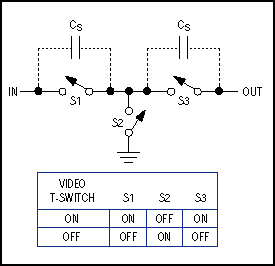
Figure 8. The T-switch configuration attenuates RF frequencies that couple through the stray capacitance between the source and the drain of an open (off) switch.
Smaller Packages
Other advantages for CMOS analog switches include small packages, such as the 6-pin SOT23, and no mechanical parts (unlike reed relays). Maxim offers a small video switch (MAX4529) as well as a standard, low-voltage SPDT switch (MAX4544). Both come in 6-pin SOT23 packages and operate from supply voltages in the 2.7V to 12V range. The MAX4544 is the smallest SPDT analog switch currently available. See Table 2.Table 2. Small Packages
| Part Number | Function | RDS(ON) (Ω max) |
ICOM(OFF) /ID(OFF) (nA max) |
RON Flatness (Ω max) |
tON/tOFF (ns max) | Charge Injection (pC max) | Off-Isolation (dB max)/ Frequency (MHz) | Supply Voltage Range (V) | Pin- Package |
| MAX4501/2 | SPST NO/ NC | 250 | 1 | - | 75/50 | 10 | -100/0.1 | +2 to +12 | 5-SOT23-5|8-DIP/SO |
| MAX4503/4 | SPST NO/ NC | 250 | 1 | - | 150/100 | 10 | -90/0.1 | ±1 to ±6 | 5-SOT23-5|8-DIP/SO |
| MAX4514/5 | SPST NO/ NC | 20 | 1 | 3 | 150/100 | 10 | -90/0.1 | +2 to +12 | 5-SOT23-5|8-DIP/SO |
| MAX4516/7 | SPST NO/ NC | 20 | 1 | 4 | 100/150 | 20 | -86/0.1 | ±1 to ±6 | 5-/SOT23-5|8-DIP/SO |
| MAX4529 | SPST NC | 70 | 1 | 10 | 75/75 | 10 | -80/10 | ±2.7 to ±6 or +2.7 to +12 | 6-SOT23-6|8-DIP/SO//µMAX |
| MAX4544 | SPDT | 60 | 0.1 | 6 | 100/75 | 5 | -76/-90 | +2.7 to +12 | 6-SOT23-6|8-DIP/SO/µMAX |
| MAX4707 | 1 SPDT NO | 3 | 1 | 0.85 | 20/15 | 5 | -82/1 | +1.8 to +5.5 | 5-SC70 6-SC70 |
| MAX4719 | 2 SPDT | 20 | 0.5 | 1.2 | 80/40 | 18 | -80/1 | +1.8 to +5.5 | 10-µMax 12-USCP |
| MAX4723 | 2 SPDT NO/NC | 4.5 | 0.5 | 1.2 | 80/40 | 18 | -80/1 | +1.8 to +5.5 | 8-µMax 9-USCP |
| MAX4730 | 1 SPDT | 5.5 | - | 0.95 | 45/26 | 3 | -67/1 | +1.8 to +5.5 | 6-SC70 |
| MAX4733 | 2 SPDT NO/NC | 50 | 0.1 | 9 | 150/60 | 7.5 | -72/1 | +2 to +11 | 8-µMax 9-/USCP |
As mentioned earlier, Maxim offers many variations of popular analog switches like the CD4066, including a family of low-cost quad analog switches (MAX4610-MAX4612). The MAX4610 is a pin-compatible improvement over the industry-standard 4066, but with lower supply voltage (as low as 2V) and higher accuracy: channel matching to within 4Ω maximum and channel flatness to within 18Ω maximum. This family of parts offers three switch configurations, and their lower on-resistance (<100Ω at 5V) suits low-voltage applications. A tiny 14-pin TSSOP package (6.5 x 5.1 x 1.1mm ³ max) solves the problem of board space.
ESD-Protected Switches
Based on the success of Maxim's ESD-protected interface products, ±15kV ESD protection was added to some of the more recent analog switches (Table 3). Maxim now offers the first switches with ±15kV ESD protection per IEC 1000-4-2 Level 4 (the highest level). All analog inputs are ESD-tested using the Human Body Model, as well as the Contact and Air-Gap Discharge methods specified in IEC 1000-4-2. The MAX4551/MAX4552/MAX4553 switches are pin-compatible with many standard quad-switch families such as the DG201/211 and the MAX391 types. To augment standard multiplexer families like the 74HC4051 and the MAX4581, Maxim also released ESD-protected multiplexers. You no longer need to use costly TransZorbs&8482; to protect your analog inputs.Table 3. ± 15k ESD per IEC 1000-4-2, in 16-pin DIP, SO, and QSOP Packages
| Part Number | Function | RDS(ON) (Ω max) |
ICOM(OFF) /ID(OFF) (nA max) |
RON Match (Ω max) |
RON Flatness (Ω max) |
tON/tOFF (ns max) | Charge Injection (pC typ) | 100kHz OFF-Isolation/Crosstalk (dB typ) | Supply Voltage Range (V) |
| MAX4551 | 4 SPST NO | 120 | ±1 | 4 | 8 | 110/90 | 2 | -90/-90 | ±2 to ±6 or +2 to +12 |
| MAX4552 | 4 SPST NC | 120 | ±1 | 4 | 8 | 110/90 | 2 | -90/-90 | ±2 to ±6 or +2 to +12 |
| MAX4553 | 4 SPST NO, NC | 120 | ±1 | 4 | 8 | 110/90 | 2 | -90/-90 | ±2 to ±6 or +2 to +12 |
| MAX4558 | 8 x 1 Mux | 160 | ±1 | 6 | 8 | 150/120 | 2.4 | -96/-93 | ±2 to ±6 or +2 to +12 |
| MAX4559 | Dual 4 x 1 Mux | 160 | ±1 | 6 | 8 | 150/120 | 2.4 | -96/-93 | ±2 to ±6 or +2 to +12 |
| MAX4560 | 3 SPDT | 160 | ±1 | 6 | 8 | 150/120 | 2.4 | -96/-93 | ±2 to ±6 or +2 to +12 |
| MAX4569 | 1 SPST NO | 70 | ±0.5 | 2 | 4 | 150/80 | 6 | -75 | ±2 to ±6 +2 to +12 |
| MAX4577 | 2 SPST | 70 | ±0.5 | 2 | 4 | 150/80 | 4 | -75/90 | ±2 to ±6 +2 to +12 |
| MAX4620 | 4 SPST NO | 70 | ±0.5 | 2 | 4 | 150/80 | 5 | -75/90 | ±2 to ±6 +2 to +12 |
Fault-Protected Switches
As mentioned under "Signal Handling" above, the supply-voltage rails for an analog switch restrict the allowed range for input signal voltage. Normally this restriction is not a problem, but in some cases the supply voltage can be turned off with analog signals still present. That condition can permanently damage the switch, as can transients outside the normal range of the power supply. Maxim's fault-protected switches and multiplexers guarantee overvoltage protection of ±25V and power-down protection of ±40V, along with rail-to-rail signal handling and the low on-resistance of a normal switch (Figure 9). The input pin, moreover, assumes a high impedance during fault conditions regardless of the switch state or load resistance. Only nanoamperes of leakage current can flow from the source.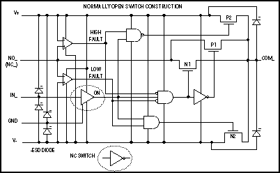
Figure 9. This internal structure shows the special circuitry in a fault-protected analog switch.
If the switch (P2 or N2) is on, the COM output is clamped to the supply by two internal 'booster' FETs. Thus, the COM output remains within the supply rails and delivers a maximum of ±13mA depending on the load, but without a significant current at the NO/NC pin. The fault-protected switches, MAX4511/MAX4512/MAX4513, are pin-compatible with the DG411-DG413 and DG201/DG202/DG213 types (Table 4). Note that signals pass equally well in either direction through an ESD- and fault-protected switch, but these protections apply only to the input side.
Table 4. Fault Protection with Rail-to-Rail Signal Swings
| Part Number | Function | RDS(ON) (Ω max) |
ICOM(OFF) /ID(OFF) (nA MAX) |
RON Match (Ω max) |
tON/tOFF (ns max) |
Overvoltage Supplies ON/OFF (V) |
Charge Injection (pC max) |
Supply Voltage Range(V) |
Pin- Package |
| MAX4505 | 1 Line Protector | 100 | ±0.5 | - | - | ±36/±40 | - | ±8 to ±18 or +9 to +36 | 5-SOT|8-µMAX |
| MAX4506 | 3 Line Protector | 100 | ±0.5 | 7 | - | ±36/±40 | - | ±8 to ±18 or +9 to +36 | 8-DIP/SO/CERDIP |
| MAX4507 | 8 Line Protector | 100 | ±0.5 | 7 | - | ±36/±40 | - | ±8 to ±18 or +9 to +36 | 18-/DIP/SO/20-SSOP |
| MAX4508 | 8 x 1 Mux | 400 | ±0.5 | 15 | 275/200 | ±25/±40 | 10 | ±4.5 to ±20 or +9 to +36 | 16-DIP/SO |
| MAX4509 | 4 x 1 Mux | 400 | ±0.5 | 15 | 275/200 | ±25/±40 | 10 | ±4.5 to ±20 or +9 to +36 | 16-DIP/SO |
| MAX4511 | 4 SPST NO | 160 | ±0.5 | 6 | 500/400 | ±36/±40 | 5 | ±8 to ±18 or +9 to +36 | 16-DIP/SO/CERDIP |
| MAX4512 | 4 SPST NC | 160 | ±0.5 | 6 | 500/400 | ±36/±40 | 5 | ±8 to ±18 or +9 to +36 | 16/-DIP|16/SO|16/CERDIP |
| MAX4513 | 4 SPST NO, NC | 160 | ±0.5 | 6 | 500/400 | ±36/±40 | 5 | ±8 to ±18 or +9 to +36 | 16-DIP/SO/CERDIP |
| MAX4533 | 4 SPDT | 175 | ±0.5 | 6 | 250/150 | ±25/±40 | 5 | ±4.5 to ±20 or +9 to +36 | 20-Wide SO/SSOP |
| MAX4631 | 2 SPST NO | 85 | ±0.5 | 6 | 150/100 | ±36/±40 | 10 | ±4.5 to ±20 or +9 to +36 | 16-DIP/SO/CERDIP |
| MAX4632 | 2 SPDT | 85 | ±0.5 | 6 | 150/100 | ±25/±40 | 10 | ±4.5 to ±20 or +9 to +36 | 16-DIP/SO/CERDIP |
| MAX4633 | 2 DPST NO | 85 | ±0.5 | 6 | 150/100 | ±36/±40 | 10 | ±4.5 to ±20 or +9 to +36 | 16-DIP/SO/CERDIP |
| MAX4510 | 1 SPST NC | 160 | ±0.5 | - | 500/175 | ±36/±40 | 5 | +9 to +36 ±4.5 to ±20 |
6-/SOT23 8-µmax |
| MAX4520 | 2 SPDT NO | 160 | ±0.5 | - | 500/175 | ±36/±40 | 5 | +9 to +36 ±4.5 to ±20 |
6-SOT23 8-µmax |
| MAX4534 | 1 2:1MUX | 275 | ±2 | 10 | 275/200 | ±25/±40 | 10 | +9 to +36 ±4.5 to ±20 |
14-TSSOP/SO/DIP |
| MAX4535 | 2 2:1MUX | 275 | ±2 | 10 | 275/200 | ±25/±40 | 10 | +9 to +36 ±4.5 to ±20 |
14-TSSOP/SO/DIP |
| MAX4711 | 4 SPST NC | 25 | ±0.5 | 1 | 125/80 | ±7/±12 | 25 | +2.7 to +11 ±2.7 to ±5.5 |
8-µMax 9-UCSP |
Force-Sense Switches
Maxim offers a family of analog switches with different switch types residing in the same package. The MAX4554/MAX4555/MAX4556 devices, for instance, are configured as force-sense switches for Kelvin sensing in automated test equipment (ATE). Each part contains low-resistance high-current switches for forcing current and higher-resistance switches for sensing voltage or switching guard signals. On-resistance for the current switches is only 6Ω, and for the sensing switches is 60Ω at ±15V supply voltages. The MAX4556 contains three SPDT switches with break-before-make action.Typical force-sense applications are found in high-accuracy systems and in measurement systems that involve long distances (Figure 10). For 4-wire measurements, two wires force a voltage or current to the load, and two other wires connected directly to the load sense the load voltage.
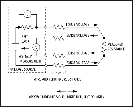
Figure 10. With the 4-wire technique, two wires force and two other wires sense the measured voltage.
Alternatively, a 2-wire system senses load voltage at the ends of the force wires opposite the load. Load voltage is lower than the source voltage, because the forcing voltage or current causes a voltage drop along the wires. Longer distance between source and load, larger load current, and higher conductor resistance all contribute for this degradation. The resulting signal reduction can be overcome by using a 4-wire technique in which the two additional voltage-sensing conductors carry negligible current.
Force-sense switches simplify many applications, such as switching between one source and two loads in a 4-wire system. They are suitable for use in high-accuracy measurement systems, such as nanovoltmeters and femtoammeters, and for 8- or 12-wire force-and-sense measurements using the guard wires of triax cables. For more information, please see the MAX4554/MAX4555/MAX4556 data sheet.
Multiplexers
In addition to switches, Maxim makes a number of multiplexers (muxes). A mux is a special version of a switch in which two or more inputs are selectively connected to a single output. A mux can be as simple as an SPDT switch or come in 4:1, 8:1, 16:1, or even dual 4:1 and 8:1 combinations. The digital control for these higher order muxes is similar to a binary decoder with three digital inputs required to select the appropriate channel.A demultiplexer is basically a mux used backwards. That is, one input connects to two or more outputs based on the decoded address data.
There are, finally, cross-point switches. A cross-point switch is usually an M x N device, whereby any or all of M inputs may be connected to any or all of N outputs (and vice versa).
Calibration Multiplexers
Calibration multiplexers (cal-muxes) are used in precision ADCs and other self-monitoring systems. They combine different components in one package: analog switches for generating accurate voltage ratios from an input reference voltage; internal precision resistor-dividers; and a multiplexer for selecting between different inputs. Maxim introduced this combination of functions in a single package.Two of these devices (MAX4539 and MAX4540) can balance two major errors associated with an ADC system: offset and gain error. Using the internal precision voltage-dividers, these devices measure gain and offset in a few steps, controlled trough the serial interface of a microcontroller. The reference ratios 15/4096 and 4081/4096 (with respect to the external reference voltage) are accurate to 15 bits. The ratios (5/8)(V+-V-) and V+/2 are accurate to 8 bits.
The cal-mux first applies one-half the supply voltage to verify that power is present. The system then measures zero offset and gain error, and forms an equation to correct the subsequent readings. Zero input voltage, for example, should produce a digital zero output. The cal-mux calibrates for offset error by applying a very small input voltage of 15/4096 referred to (VEFHI-REFLO). For a 12-bit ADC with 4.096V reference, 15/4096 equals 15mV and also 15 LSBs. The digital output therefore should be binary 000000001111. To measure offset error, the microcontroller simply records the difference between binary 000000001111 and the ADC's actual output.
To measure gain error, the cal-mux applies a voltage of 4081/4096 referred to (VREFHI-VREFLO). The microcontroller then records the difference between binary 111111110000 and the ADC's digital output. Knowing the ADC's offset and gain error, the system software constructs calibration factors that adjust the subsequent outputs to produce correct readings. The cal-mux then serves as a conventional multiplexer, but with the ability to recalibrate the system periodically.