Current-mode data transmission is the preferred technique in many environments, particularly in industrial applications. This application note describes the design of a 4-20mA current loop.
Most systems employ the familiar 2-wire, 4-20mA current loop, in which a single twisted-pair cable supplies power to the module and carries the output signal as well. The 3-wire interface is less common but allows the delivery of more power to the module electronics. A 2-wire system provides only 4mA at the line voltage (the remaining 16mA carries the signal). Current loops offer several advantages over voltage-mode output transducers:
- They don't require a precise or stable supply voltage.
- Their insensitivity to IR drops makes them suitable for long distances.
- A 2-wire twisted-pair cable offers very good noise immunity.
- The 4mA of current not required for information transfer serves two purposes: it can furnish power to a remote module, and it provides a distinction between zero (4mA) and no information (no current flow).
Basic 2-wire, 4-20mA Circuit
Konrad and Ashaur¹ have demonstrated the compensation of piezoresistive sensors using new semiconductor components such as the MAX1450, MAX1457, MAX1458, and MAX1459. Operating in the standard ratiometric configuration, these and similar other ASICs provide first-order electronic compensation of temperature effects (the MAX1457 compensates higher-order effects as well). They also achieve typical accuracies better than ±1% over temperature (0.1% for the MAX1457).A standard ratiometric circuit compensates the sensor to an offset of 0.5V and a span of 4.0V over the operating temperature range. Because current-mode applications require a 4mA offset and 16mA span, you must translate a voltage output to current when configuring a ratiometric 4-20mA circuit. This app note presents the circuit details and results obtained from a current-loop configuration based on the MAX1459 sensor-signal conditioner.
We start with a standard ratiometric circuit and show how to modify it for current-mode applications. In principle we need only add a voltage regulator, which converts the 10-to-32V loop voltage to a fixed 5V for operating the MAX1459. We also use the MAX1459's uncommitted auxiliary amplifier to make a voltage-to-current converter, using an external transistor and some discrete passive components.
Figure 1 shows the circuitry required in addition to that implementing a standard ratiometric version of the MAX1459 circuit. The voltage regulator can be any low-cost device whose quiescent current is sufficiently low for the 4mA budget. Resistors Rx and Ry are optional. Ry limits the transistor's base current, primarily during power-up and large transients.
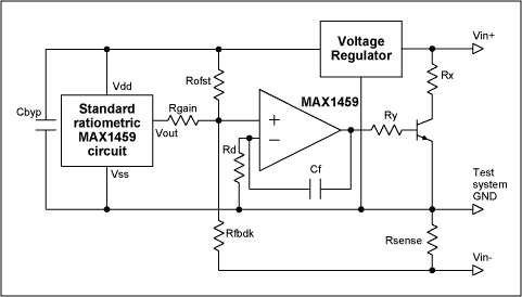
Figure 1. This circuit shows the basic functional blocks of a 4-20mA transmitter.
Rx is more strongly recommended, because it protects the transistor from large transient currents during power-up and during voltage transients. Rx also ensures reliability by helping to protect the transistor during high-temperature operation. By sharing load power it maintains the transistor junction temperature in a safe region. The value of Rx is determined by the minimum operating voltage (Vin), the maximum operating current (20mA), the voltage drop across Rsense, and the transistor's Vce saturation voltage. For applications in which the minimum Vin is low, it may be necessary to eliminate Rx altogether. Capacitor Cf is recommended for compensating the amplifier.
4-20mA Equations
We begin by noting that all system currents must flow through Rsense and Rfdbk. The ratio of these resistors should be chosen so most of the current flows through Rsense, yet the voltage drop across it is small. Selecting Rfdbk much larger than Rsense simplifies the equations somewhat, and should also allow us to ignore the small parasitic current flowing through Rfdbk. On this basis, we can select convenient values for Rsense and Rfdbk.The MAX1459 output (Vout) is calibrated for 0.5V at minimum pressure and 4.5V at maximum pressure. Thus, ΔVout = 4V. The transmitter offset current is 4mA, the FSO current is 16mA, and Vdd = 5V. Because the Rd current is negligible, current through Rfdbk is the sum of currents flowing through Rofst and Rgain. The current I ranges between 4mA and 20mA. Therefore,

Solving for Rofst,

Next, determine the value for Rgain by noting that a 4V FSO across Rgain (ΔVout) must add 16mA across Rsense. Therefore,

Solving for Rgain;

Solutions
Figure 2 is a more detailed version of Figure 1. Choosing Rsense = 50Ω makes that resistor drop 1V at 20mA. Then, choosing Rfdbk = 100KΩ establishes an Rsense/Rfdbk ratio that limits the equation error to only 0.05% (the equations do not account for the effect of Rfdbk in the current loop). We can neglect this Rfdbk effect, because the FSO and offsets are adjusted with DACs internal to the MAX1459. We next assume a 10V minimum operating voltage and choose Rx = 390Ω. At maximum current, this leaves 2.2V of headroom for Rsense and the transistor Vce drop. Select 5KΩ for the optional Ry. Finally, determine Rofst and Rgain using Equations 1-2 and 1-4. Table 1 summarizes the resulting component values.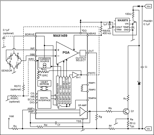
Figure 2. Circuitry internal to the MAX1459 IC helps to understand operation of the Figure 1 circuit.
Table 1. Component Values for 4-20mA Applications
| Parameter | Value | Comments |
| Supply (min) | 10V | Determined by regulator dropout and Rx |
| Supply (max) | 32V | Limited by regulator and transistor |
| I Minimum | 4mA | Zero pressure reference output |
| I Mid-scale | 12mA | Mid-scale current output |
| I Maximum | 20mA | Full-scale pressure output |
| Rsense | 50Ω | 1 volt drop at 20mA |
| Rfdbk | 100KΩ | Should be > than Rsense |
| Rofst | 5MΩ | Determines current loop Offset value |
| Rgain | 500KΩ | Determines current loop gain value |
| Rx | 390Ω | Protects the output transistor |
| Ry | 5KΩ | Optional component |
| Cbyp | 2.2µF | Reduces digital noise in loop output |
| Cc | 0.1µF | Recommended for stability over temp |
| Rd | 100KΩ | Recommended for stability over temp |
The values determined for Rofst and Rgain are ideal values, and they provide very little extra range to accommodate variations in the component values. In practice, it is preferable to obtain a larger adjustment range for FSO by lowering the value of Rgain. The value of Rofst should also be changed by a small amount. This approach allows use of low-accuracy resistors, and their TC is of little concern because the MAX1459 compensates for the collective effect of temperature on the resistors.
Because line- and load-regulation errors cannot be compensated by the MAX1459, the basic regulator requirements are low line-regulation error, and (to a lesser extent) low load-regulation error. To meet the 4mA budget, the quiescent operating current should be less than 500µA. Voltage-calibration accuracy and temperature coefficient are of secondary importance because the MAX1459 compensates these parameters. The regulator's maximum input voltage should be greater than the maximum loop-supply voltage (Vin).
A power-supply bypass capacitor Cbyp (in addition to the one required within the standard ratiometric circuit) has been added to prevent the noise of digital activity in the MAX1459 EEPROM from appearing on the output-current loop. This capacitor value depends on the circuit layout and the regulator characteristics. The EEPROM supply can be separated from the MAX1459 with an RC network consisting of a large value capacitor and a small value resistor.
The test system ground return should be at the junction of Rsense and the emitter of the output transistor. This node is equivalent to the MAX1459's Vss node. Because the ground return is floating, it must not be connected in parallel with other devices in a test system with multiple transducers. Nor should loop current be measured in the presence of digital activity between the MAX1459 and the test system. DIP relays are recommended for selecting and deselecting both the ground return and the digital lines required for programming individual modules.
Results obtained after compensating the sensor are shown in Figure 3. Large raw sensor errors are temperature compensated to within ±1%. The compensation procedure assumes an output voltage from the pressure transducer that is ratiometric to the supply voltage (the MAX1459 current source). This procedure requires a minimum of two test pressures (zero and full scale) at two arbitrary test temperatures. Ideally, the two temperatures are those for which we wish to perform a best linear-fit compensation.
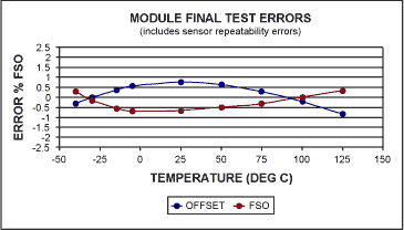
Figure 3. Post-compensation results.
¹B. Konrad and M. Ashaur, "Demystifying Piezoresistive Pressure Sensors," Sensors, July 1999, pgs.12-25.