When we want to capture a low level, long duraTIon signal riding on a much higher DC level, we need to have adequate resoluTIon of the input step and the capacity to offset the large DC level. This is a funcTIon that can be found in the oscilloscope, but with limited range. This application note outlines the ways to perform this measurement.
Low Input DC Voltage
A long duration time waveform looks like Figure 1 when the signal is observed on the oscilloscope with AC coupling. This distorted waveformis caused by the high pass filter formed by the input impedance at the input of the scope. The correct way to measure this is to input the signal with DC coupling and to use the 'offset' function on the scope to bring the scope trace to within range. This method is useful when the DC level of the input voltage is low, so that the 'offset' range of the oscilloscope is wide enough to capture the waveform.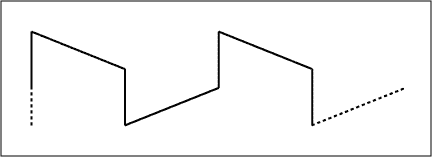
Figure 1. AC coupling a low frequency square waveform.
High Input DC Voltage, Low Level Signal Change
When the DC level of the input signal is high in comparison with the signal level, e.g. a 10mV step change on a 5V input, the offset function on the scope may not have a wide enough range to bring the waveform in with acceptable resolution on the display. A level shifting circuit, as depicted in Figure 2, can be used to manipulate the input signal to be readily observed on the oscilloscope. U1 is a general-purpose low offset operational amplifier. Apply a negative voltage equal in magnitude to the input voltage to the summing input of the op-amp through the resistor R2. Observe the output with DC coupling. Note that the output is inverted to the input as the amplifier has a gain of -10. Use the 'invert' function of the oscilloscope to invert the trace as needed. The driving capability of most function generators is about 5mA. The current drawn from the function generator in Figure 2 is 2.5mA (5V/2kΩ). Increase R1 when the input DC level is higher than 5V. Set R2 = R1 and R3 = 10 × R1 to maintain the same summing function and gain. The benefit of this circuit is that it amplifies the change of signal level. The drawback is that current is drawn from the signal source and that the output is inverted.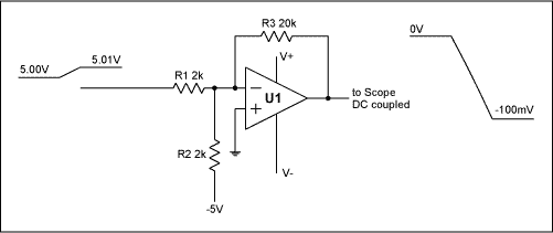
Figure 2. Level shifting with gain.
High Input DC Voltage, High Level Signal Change
When the input signal level change is high, Figure 3 provides a circuit to conveniently observe the output. Q1 and Q2 are PNP transistors (2N2907A). U2 is a general-purpose low offset operational amplifier. With R1 = R2 the collector current of Q1 isIQ1 = (VCC - VBE) / (R3 + R2).The voltage across R4 is IQ1 × R4. Adjust R4 to cancel the DC level of the input signal. The output signal can then be monitored using DC couple on the oscilloscope. The circuit has a gain of +1. The advantage of this circuit is that the output is in phase with the input signal and draws negligible current from the signal source.
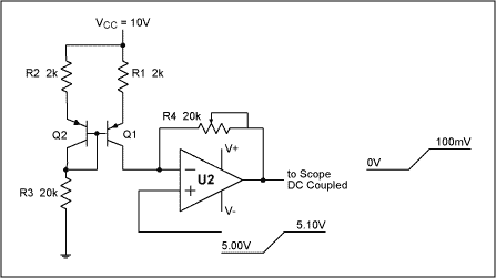
Figure 3. Level shifting with gain of 1.