General Description
The MAX5052A is a current-mode PWM controller. It contains all the necessary control circuitry required for the design of an isolated power supply. This application note describes the design of a 23W isolated power supply. The topology employed is a single transistor forward with synchronous rectification. Remote sense pins compensate for load cable voltage drops. The switching frequency of the MAX5052A is set at 262kHz and it is internally trimmed to ±12% accuracy. The MAX5052A has a maximum duty cycle of 50%.Specifications
- Input voltage 40VDC–60VDC
- Power supply dimensions: 1.79" × 0.95" × 0.60"
- Output voltage: 3.3V ±2%
- Output current: 7A
- Over-voltage 4V ±5%
- Over-current and short circuit protection
- Remote sense
- No damage should occur to the remote sense resistors if the connections of the remote sense is reversed.
- Isolation voltage, primary to secondary 1500VDC.
Circuit Operation
The input voltage is connected to the connector J2. C8 is a 1µF, 100V high frequency Ceramic capacitor, connected across the input. An external electrolytic capacitor is connected across the input of the power supply. Resistor R6 charges up the VIN bypass capacitor C2 from the input. C2 is a 4.7µF, 50V electrolytic capacitor. Once the converter starts up, capacitor C2 is bootstrapped by the bias winding. The voltage across R5 is a pulsating waveform, with a peak voltage equal to the input voltage times the turns ratio of the bias winding to the primary winding. Resistor R1 and capacitor C14 average this pulsating waveform. The diode D8 is used to prevent the capacitor C2 from discharging into the series combination of resistors R1 and R5. The bootstrapped winding voltage across C14 is proportional to the output voltage. The MOSFET Q3 is the primary switching FET. R14 is the current sense resistor. Resistor R7 and R12 form the under-voltage lockout set point of the power supply. With the given values, the turn-on voltage is 39V.Synchronous rectification on the secondary side is used to increase the power supply efficiency. The gate charge retention scheme is used to guarantee gate drive voltage on the freewheeling MOSFET when the transformer winding voltage has gone to zero. In a dc-dc converter with a two-to-one line swing of the input voltage, this time can be 50% of the duty cycle, or higher, at the highest input voltage. This is true in the case where the reset winding has the same number of turns as the primary power winding and the reset winding is returned to the input via a reset diode. In the current application the input voltage was changing from 40V to 60V.
The forward path synchronous MOSFET Q1 is turned on when the transformer voltage on the secondary goes positive and is turned off when the main switching FET is turned off. The freewheeling MOSFET Q4 is turned on when switch Q3 is turned off and the transformer voltage reverses. Once the transformer voltage goes to zero, MOSFET Q2 is kept on because there is no discharge path on the gate of Q2. When the primary switching FET Q3 is turned on, the MOSFET Q4 is turned on and this discharges Q2 rapidly resulting in the turn of off Q4.
U1 is the secondary feedback opto-coupler that sends the feedback signal across the isolation barrier. U5 is an opto-triac which shuts off the PWM controller in case of an over-voltage by discharging C2 and keeping it discharged until the input power is recycled. R23 and R18 are the positive and negative remote sense resistors. When the power supply hits the current limit the duty cycle will pitch back, causing the output voltage to drop. This will also cause the voltage across C14 to drop. Since the voltage across C14 is directly proportional to the output voltage, a heavy overload on the output would cause a sufficient drop in the bias voltage on C14 such that the voltage on C2 would drop below 9.9V causing the controller to shut down and go into a hiccup mode of operation, thus causing a reduction in the RMS short circuit current. This mode of operation of the power supply allows us to short the power supply output without overheating the output semiconductors and inductor. Diodes D9 and D10 provide an alternate path for the current when the remote sense wires are crossed. This will cause the output to be short-circuited by diodes D9 and D10 and will put the power supply into the hiccup mode of operation. This prevent the resistors R18 and R23 from opening up due to excessive current.
Performance Data
Peak-to-peak ripple at an input voltage of 60V. Output 3.3V at 7AMeasured peak-to-peak ripple was 124mV at 20MHz bandwidth.
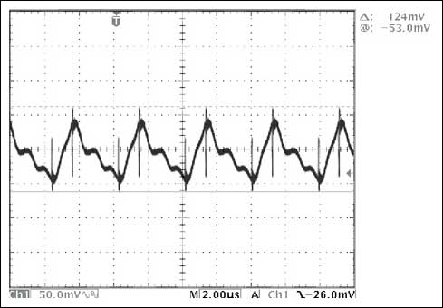
Figure 1.
Peak-to-peak ripple at an input voltage of 48V. Output 3.3V at 7A
Measured peak-to-peak ripple was 100mV with the bandwidth set at 20MHz.
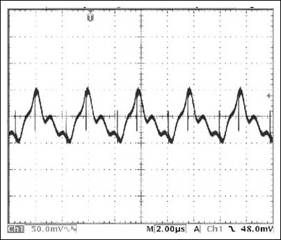
Figure 2.
The output ripple and noise could be further improved by increasing the number of output capacitors or by using output capacitors with lower ESR.
Transient Response
Transient response measured at 48V input and a load step decrease from 5.25A to 3.5A.The peak positive excursion was measured at 160mV.
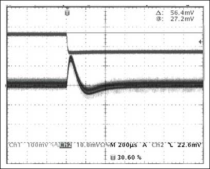
Figure 3.
Transient response measured at 48V input and a load step increase from 3.5A to 5.25A.
Here the peak negative excursion was 220mV. The difference in behavior can be attributed to the change in crossover frequency and the phase margin at 3.5A and 5.25A.
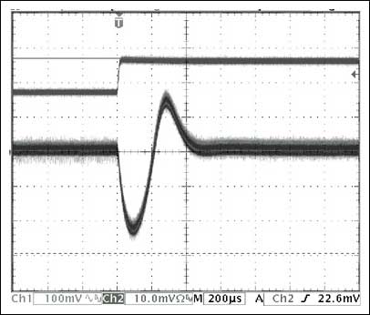
Figure 4.
Table 1. Efficiency Data
|
|
|
|
|
|
| 40V | 0.32352A | 3.2685V | 3.5006A | 88.4% |
| 40V | 0.45893A | 3.2675V | 5.0111A | 89.2% |
| 40V | 0.6485A | 3.2653V | 7.0111A | 88.25% |
| 48.1V | 0.2770A | 3.2663V | 3.5332A | 86.4% |
| 48.1V | 0.38655A | 3.2663V | 5.0116A | 88.0% |
| 48.1V | 0.54735A | 3.26652V | 7.044A | 87.6% |
| 60V | 0.22912A | 3.2657V | 3.5010A | 83.2% |
| 60V | 0.31670A | 3.2657V | 5.0116A | 86.1% |
| 60V | 0.44163A | 3.2647V | 7.011A | 86.4% |
PCB Information
The PCB is compact and it has components on both sides. The dimensions along with the component placement are shown below.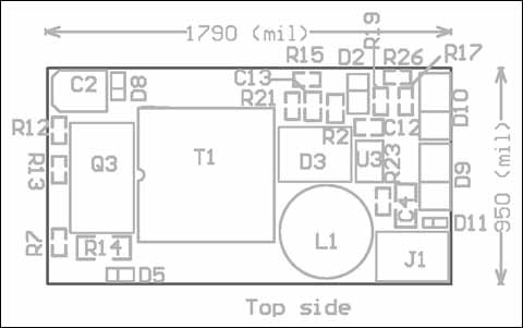
Figure 5.
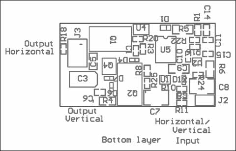
Figure 6.
Table 2. Component List for 23W Power Supply
|
|
|
|
| C1 |
|
Ceramic capacitor, 1000pf, 25V, X7R (0402) |
| C2 |
|
Electrolytic capacitor, 4.7µF, 50V Panasonic EEVFK1H4R7R |
| C3 |
|
SP capacitor, 180µF, 6.3V Panasonic EEFUEOJ181R |
| C4, C5 |
|
Ceramic capacitor, 4.7µF, X5R, 6.3V (0805) |
| C6 > |
|
Ceramic capacitor, 680pF, 50V, X7R (0603) |
| C7 |
|
Ceramic capacitor, 4700pF, 250vac, X7R(1812) Murata GA243DR7E2472MW01L |
| C8 |
|
Ceramic capacitor, 1µF, 100V, X7R (1812) |
| C9 |
|
Ceramic capacitor, 1µF, 16V, X7R (0805) |
| C10 |
|
Ceramic capacitor, 100pF, 50V, COG (0402) |
| C11, C12 |
|
Ceramic capacitor, 0.47µF, 10V, X5R (0603) |
| C13 |
|
Ceramic capacitor, 1µF, 10V, X5R (0603) |
| C14 |
|
Ceramic capacitor, 0.1µF, 50V, X7R (0603) |
| C15 |
|
Ceramic capacitor, 4700pf, 50V, X7R (0402) |
| C16 |
|
Ceramic capacitor, 0.047µF, 16V, X7R (0402) |
| R1 |
|
Resistor 220Ω, 5%, (0603) |
| R2 |
|
Resistor 4.7Ω, 5% (0603) |
| R3, R11 |
|
Resistor 3.30kΩ, 1% (0402) |
| R4 |
|
Resistor 10Ω, 5% (0805) |
| R5 |
|
Resistor 3.3kΩ, 5% (1206) |
| R6 |
|
Resistor 82kΩ, 1% (0805) |
| R7 |
|
Resistor 274kΩ, 1% (0603) |
| R8 |
|
Resistor 221Ω, 1% (0603) |
| R9 |
|
Resistor 4.99kΩ, 1% (0402) |
| R10, R13 |
|
Resistor 1kΩ, 1% (0402) |
| R12 |
|
Resistor 10kΩ, 1% (0402) |
| R14 |
|
Resistor 0.15Ω, 1% (1206) |
| R15 |
|
Resistor 36kΩ, 1% (0402) |
| R16 |
|
Resistor 330Ω, 1% (0402) |
| R17 |
|
Resistor 205Ω, 1% (0402) |
| R18, R23 |
|
Resistor 10Ω, 5% (0402) |
| R19 |
|
Resistor 124Ω, 1% (0402) |
| R20 |
|
Resistor 16.2kΩ, 1% (0402) |
| R22 |
|
Resistor 100Ω, 5% (0402) |
| R24 |
|
Resistor 22Ω, 5% (0402) |
| R25 |
|
Resistor 2.2kΩ, 5% (0402) |
| R26 |
|
Resistor 1MΩ, 5% (0402) |
| R27 |
|
Resistor 10Ω, 5% (0603) |
| R28 |
|
Resistor 68Ω, 5% (0402) |
| T1 |
|
Power transformer, Transpower TTI8619 |
| Q1, Q2 |
|
N-channel MOSFET 20V (DPAK) Vishay SUD70N02-09 |
| Q3 |
|
N-channel MOSFET 150V (DPAK) Fairchild Semi FDD120AN15A0 |
| Q4 |
|
N-channel MOSFET 30V, SOT23 Fairchild NDS351AN |
| L1 |
|
Choke 4.7UH, Coilcraft DR0810-472 |
| D1, D5 |
|
Diode 200V, 200mA Panasonic MA115CT |
| D2 |
|
Signal diode 100mA 75V Diodes Inc 1N4148W |
| D3 |
|
Schottky diode 8A, 35V (PowerMite) Diodes Inc SBM835L |
| D4, D6, D7, D11, D12 |
|
Schottky diode 30V, 100mA Panasonic MA2S784 |
| D8 |
|
Diode 100V, 200mA Panasonic MA111CT |
| D9, D10 |
|
Schottky diode, 3A, 20V Diodes Inc B320A |
| U1 |
|
Optocoupler Fairchild HMHA2801 |
| U2 |
|
Current mode PWM Maxim MAX5052AEUA |
| U3, U4 |
|
Precision reference 1.25V, 1% (SOT23-5) Texas Instruments TLV431ACDBVR |
| U5 |
|
Opto-coupler triac Fairchild MOC3023 |
For Larger Image
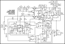
Figure 7. Schematic of 23W power supply.