Design ConsideraTIons for Dallas Semiconductor Real-TIme Clocks
Abstract: A real-TIme clock (RTC) allows a system to synchronize or TIme-stamp events to a time reference that can be easily understood by the user. Because RTCs are used in an increasing number of applications, designers should familiarize themselves with these RTCs to avoid design problems. This application note provides a basic overview of RTC operation, design issues, and troubleshooting techniques.
Selecting an Interface
Real-time clocks (RTCs) are available in a wide range of bus interfaces. Serial interfaces include I²;C, 3-wire, and Serial Peripheral Interface (SPI™). Parallel interfaces include mux-bus (multiplexed data and address bus) and designs with separate address and bytewide data inputs.
The choice of interface is often determined by the type of processor being used. Many processors include I²C or SPI interfaces. Others, such as 8051 processors and their derivatives, support multiplexed address and data buses. Timekeeping NV RAMs use the same control signals as SRAMs, to which many processors provide an easy interface, and include battery-backed RAM in various densities. Finally, phantom clocks "hide" behind battery-backed RAM and use a 64-bit software protocol to gain access to the clock. A phantom clock can therefore provide time and date infromation without using any memory space.
Battery Backup Function
In some applications such as VCRs, the time and date information will be lost if power is removed. Other applications require that the time and date remain valid even if the main power supply is off. To keep the clock oscillator running, a primary or secondary battery or a super capacitor may be used. In this case, the RTC must be able to switch between the two power supplies.
If a primary battery, such as a lithium coin cell, is used for backup, the RTC should be designed to draw as little power as possible when running from the battery. In this situation the RTC will switch its internal supply bus to the battery and go into a low-power mode. Communications between the microprocessor and the RTC are usually locked out (often called write protect) to keep the battery current at a minimum and to prevent data corruption. The VCC volt1age level at which communications is locked out is usually defined in the data sheet as VTP (Trip Point Voltage).
Many clocks include an oscillator control bit, usually called the clock halt (CH) or enable oscillator (EOSC) bit. This bit is usually located in bit 7 of the seconds register, or in a control register. In almost all clocks with this bit, it is preferable that the oscillator be off when the battery is initially attached. This conserves the battery until the system is powered up. It also allows the system designer to set up a manufacturing flow so that no battery current is drawn after a fresh lithium battery is installed.. When the end user first powers the system, the firmware/software should start the oscillator and prompt the user for the time and date.
Most Dallas Semiconductor products that include a battery input pin include on-chip reverse charging protection circuitry. Regulatory agency data and Conditions of Acceptability information can be found at UL Recognition.
Lithium batteries are normally rated to operate from -40°C to +85°C. The battery should never be exposed to temperatures above +85°C. Packages that include the battery and have exposed battery pins, such as the SmartSockets, should never be water washed. Water washing will short the battery terminals, and therefore draini the batteries.
Clock Modules, Freshness Seal and Shelf Life
The majority of the current consumed by a clock while in battery-backed mode is from the oscillator. All clock modules with embedded crystals and batteries are shipped from the factory with the oscillator disabled. While the oscillator is disabled, the battery current is less than the self-discharge of the battery, or about 0.5% per year at room temperature.
Some timekeeping NV RAM modules use a clock-controller IC and a SRAM. The oscillator is disabled and the SRAM is electrically disconnected from the battery when shipped from the factory. The battery will be connected to the SRAM after VCC is removed for the first time. This function is often called "freshness seal," and is used to conserve the battery until the module is first used. Other timekeeping NV RAM modules are monolithic (controller and SRAM in one IC) and require no freshness seal.
Module Packages
Timekeeping NV RAMs, mux-bus clocks, and some watchdog and phantom clocks are available in module and/or PowerCap packages. Modules include an embedded 32,768Hz crystal and a lithium battery, making PCB design easier. However, crystals and batteries cannot tolerate the temperatures encountered during the reflow process. Consequently, modules can be attached manually or inserted in a socket after reflow. Modules can also be attached to the PCB using wavesolder, as long as the lithium battery is not exposed to temperatures above +85°C.
PowerCap products use a two-piece construction to provide a device that can be surface-mounted using the reflow process. The module base, containing the RAM and clock, is mounted to the board using standard reflow techniques. The PowerCap top, containing the heat-sensitive battery and crystal, is snapped onto the base after soldering.
Clock Formats
There are three major data formats used in RTCs: binary-coded decimal (BCD), binary with separate registers for the month, date, year, etc., and elapsed-time counters.
BCD
The BCD format is the most common. One reason for its popularity is that the time and date can be easily displayed in a human-readable format with no "conversion." Each 8-bit register represents two digits (one nibble per digit). Each 4-bit nibble can hold the binary representation of the digits 0 through 9. An example of the register map for a typical BCD format clock is shown in Figure 1.
Since some of bits are not needed for a particular time or date field, those bits can be used for special functions, general-purpose read/write bits, or can be hardwired to read back as always one or zero, depending upon the design. In Figure 1, bit 7 of the seconds register is used for the clock halt (CH) bit. (See the DS1307 data sheet for an example.)
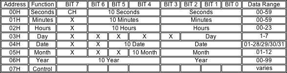
Figure 1. Typical time and date register map (BCD format).
Binary
The second clock format is the binary format (Figure 2), with separate registers like the BCD format. The binary format is normally a programmable option on some clocks with the BCD format. (See the DS12885 data sheet for an example of this format.)
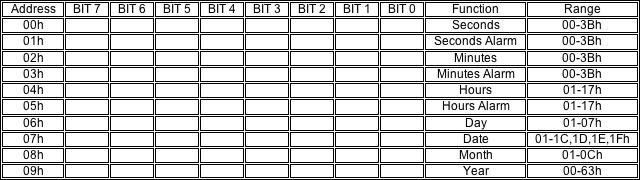
Figure 2. Typical time and date register map (binary format).
Elapsed-Time Counter
The elapsed-time counter (ETC) uses a single, multibyte register representing the time in seconds from some reference point (zero epoch). A common value is 00:00:00 January 1, 1970 GMT. The binary value in the register then represents the elapsed time from that point. Software routines must be used to convert the 32-bit value to a readable time and date, and to convert user entries to a binary value. The C ctime() function converts the elapsed time, in seconds, to a date/time string.
Application note #511, Using the DS1672 Low-Voltage Serial Timekeeping IC, presents example routines for converting elapsed-time values to and from date strings. The DS1318 is a 44-bit ETC. The lower 12 bits provide sub-second resolution, to 244µs. The upper 32-bits increment once-per-second, as described above. See application note 2740, Accessing the DS1318 Clock Registers for an example application.
ETC clocks are useful when the clock is needed to measure the time between two events. Calculating the time elapsed between two events requires subtracting one value from another, while a BCD-formatted RTC would require more complex conversion routines.
For BCD-formatted RTCs, the time and date registers are typically updated once per second. The roll-over value for the date will vary depending upon the month, and for February, by year. The day register (except for multiplexed-bus clocks) is not tied to any other register, will increment at midnight, and will roll over from 7 to 1. The programmer can select any particular day as 1, as long as the assignment is consistent throughout the program. On multiplexed-bus clocks, however, Sunday must be 1 because the day register is used for the daylight saving test. The test for daylight saving is done at midnight on the preceding midnight roll-over, which must be accounted for when testing the daylight saving function.
When changing from 12-hour mode to 24-hour mode, or from BCD to binary or binary to BCD, the time, date, and alarm registers must be re-initialized.
Crystals and Accuracy
The crystal oscillator is one of the most accurate circuits available for providing a fixed frequency. A 32,768Hz crystal is used for most RTCs. By dividing down the output of the oscillator, a 1Hz reference can be used to update the time and date. The accuracy of the RTC is dependent mainly upon the accuracy of the crystal. Tuning-fork crystals have a parabolic frequency response across temperature (Figure 3). An error of 23ppm is about 1 minute per month. For further reference, see the Real-Time Clock Calculator. Crystals are tuned to oscillate at the correct frequency under a particular capacitive load. Using a crystal tuned for a 12.5pF load on an RTC designed to present a 6pF load to the crystal will cause the clock to run too fast.
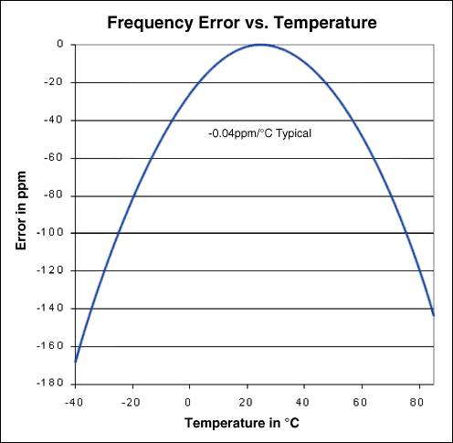
Figure 3. Crystal accuracy vs.temperature.
Crystal Connections
All Dallas Semiconductor RTC oscillators have internal bias networks. The crystal should be connected directly to the X1 and X2 pins with no additional components (Figure 4). The crystal should also be as close as possible to the X1 and X2 pins, and a ground plane should be placed beneath the crystal, X1, and X2 (Figure 5). Digital signal lines should be routed away from the crystal and oscillator pins. Low-power crystal-oscillator circuits can be sensitive to nearby RFI, which can cause the clock to run fast. Consequently, components that radiate significant levels of RFI should be shielded and located away from the crystal.
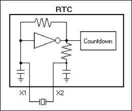
Figure 4. RTC equivelent circuit showing the internal bias network.
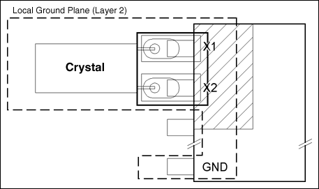
Figure 5. Typical crystal layout.
PC boards containing tuning-fork crystals, such as those used with RTCs, should not be cleaned using ultrasonics. The crystal can be damaged by resonance vibration.
Oscillator Startup Time
Oscillator startup times are highly dependent on crystal characteristics and layout. High ESR and excessive capacitive loads are the major contributors to long startup times. A circuit using a crystal with the recommended characteristics and following the recommended layout will usually start within one second.
Checking for Oscillation
When checking for oscillator operation, a designer may initially considerconnecting an oscilloscope probe to the oscillator input (X1) or output (X2) pin. That approach is not recommended with a RTC. Since the oscillator is designed to run at low power (which extends operating time from a battery), loading the oscillator with an oscilloscope probe will usually stop the oscillator. If the oscillator does not stop, the additional loading will reduce the signal amplitude, and can cause erratic operation such as varying amplitude. Oscillation should, therefore, be verified indirectly.
Oscillation can be verified several ways. One method is to read the seconds register multiple times, looking for the data to increment. On RTCs with an OSF (Oscillator Stop Flag), clearing and then monitoring this bit will verify that the oscillator has started and is continuously running. These methods will not work if the designer is troubleshooting a design and cannot communicate with the RTC. An alternate method is to check the square-wave output on RTCs with a square-wave output. Check the data sheet to verify whether the RTC must be written first to enable the oscillator and square-wave output. If the square-wave output is open-drain, a pull-up resistor must be connected between the square-wave pin and a voltage supply for proper operation. The square-wave output can also be used to verify the accuracy of the RTC, although, a frequency counter with sufficient accuracy must be used for this.
Backup Supply Input
Most Dallas Semiconductor RTCs include a backup supply input pin, which keeps the RTC running while the main supply is off. Most RTCs are designed so that a lithium coin cell can be used to power the RTC while VCC is absent.
When VCC is below the minimum operating value (VTP), the RTC disables the communications interface. This serves two purposes: it prevents accidental writes to the RTC while VCC is dropping; it reduces the power needed by the RTC to maintain oscillator, time, and date operation. Disabling access to the part when VCC is below VTP is often called "write protect." While the RTC is operating from VCC, the VBAT input will be at a high impedance. If a battery is not connected to the VBAT input, or if it is connected with diodes in series (Figure 6), the VBAT input can float high. This, in turn, can cause the RTC to go into write protect. Reverse-charging protection is provided internally on most Dallas Semiconductor RTCs, which eliminates the need for external diodes. Check the following link for information about UL recognition of the reverse-charging protection.
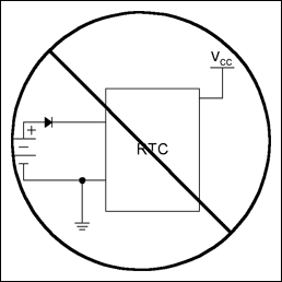
Figure 6. Incorrect battery connection.
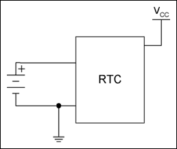
Figure 7. Correct battery connection.
Calculating Battery Life
When designing a system with an RTC, the backup power source must be selected based on the system requirements. If a system is expected to run from the main power source most of the time, the backup supply may only need to power the clock for a few hours. In other applications, the backup supply must power the clock for long periods of time.
For RTCs with a separate backup supply input (VBAT or VBACKUP), the battery backup time is calculated by dividing the battery capacity in Ampere-hours by the expected backup current. Here are two examples of how this capacity is calculated.
Example 1. A BR1225 Li+ battery has a rated capacity of 48mAH. While the DS1307 is powered by VBAT, the current drawn by the VBAT input is specified at 500nA maximum with the SQW/OUT off. Therefore, 0.048 / 500e-9 = 96,000 hours, or about 10.9 years. Note that this assumes that the battery has negligible self-discharge.
Example 2. A DS1337 is used in an application where a single battery supply powers the entire circuit. Active current (current while the I²C serial-interface is active) is rated at 150µA. Standby current, when the I²C interface is inactive, is specified at 1.5µA maximum. We will assume that for each hour that the circuit is powered, the I²C bus is active about 5% of the time and inactive the rest of the time. Therefore, the average current is expected to be 0.05 x 150µA + 0.95 x 1.5µA = 7.5µA + 1.425µA = 8.925µA per hour. This number would be added to the current drawn by the microcontroller, the I²C pullup resistors, and any other devices powered by the battery. The battery capacity would then be divided by the total current, as in Example 1, to obtain the expected battery life.
For applications that require a few hours or days of operation from the backup supply, a large capacitor or super capacitor could be used. RTCs with a built-in trickle charger support the charging of super capacitors. Refer to application note 3517, Estimating Super Capacitor Backup Time on Trickle-Charger Real-Time Clocks, and the on-line super capacitor calculator for more information.
Reading and Writing the Time and Date
Reading and writing the time and date registers is an asynchronous event, separate from the automatic update of the internal registers. Two types of read errors can occur when the time and date registers increment while being read. First, the data could change while a single register is being read, or, second, the data could change during the time between reading two registers. Assume, for example, that the clock increments from 11:59:59 to 12:00:00 during a read of the seconds, minutes, and hours registers. The time read could be 12:00:59, which is incorrect.
Some method must be used to prevent these read errors. Most Dallas Semiconductor Maxim clocks ensure that the time and date registers can be accessed without the values getting corrupted from an internal register update while the read or write is in progress.
A second set of registers (secondary buffer or "user" registers) are used on most serial clocks. When the time and date registers are accessed, the current time and date are transferred to the secondary registers. A burst read will take the data from the secondary registers, which remain unchanged while the internal registers continue to update. The next access (when CE goes active on a 3-wire device or a START on I²C interface devices occurs) will transfer the data again. When writing to the time and date registers, the internal countdown chain is reset when the seconds register is written. That allows the program almost one second in which to write the remaining time and date registers before a rollover occurs.
On timekeeping NV RAM clocks, either a transfer enable (TE) bit or (R)ead and (W)rite bits are used to "freeze" the user registers. Setting the R bit or the TE bit keeps the user registers from being updated from the main registers. Resetting the TE bit or the W bit after writing the user register loads the internal time and date registers with the values from the user registers.
The block diagram in Figure 8 shows typical functions for transferring time and date information between the internal registers and the user interface. The 32,768Hz signal from the oscillator is divided down to 1Hz by a countdown chain that has a reset input. The 1Hz signal from the countdown chain drives the BCD seconds counter/register. The ripple output from the seconds counter feeds the minutes counter/register, and so on. Changing the R and W bits in the control register synchronizes the transfer of data from the internal registers to the user registers. The Transfer Control block sends a reset to the countdown chain when transferring data from the user registers to the internal registers. This allows synchronization of the clock to an external reference to within approximately 244µs (most clocks do not reset the first three dividers, to the 4,096Hz signal; 1/4,096Hz 244µs). Most serial-interface clocks reset the countdown chain whenever the seconds register is written.
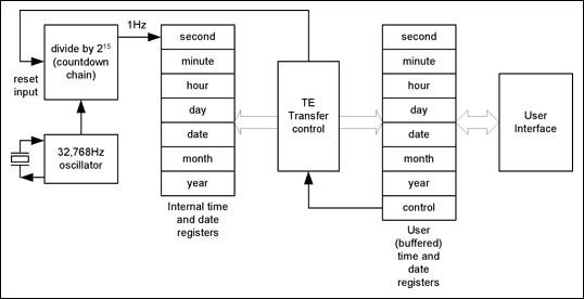
Figure 8. Block diagram showing internal and user copy of time and date registers.
On mux-bus clocks, several methods are available to ensure that the time and date registers do not change while being accessed. The following methods are available:
SET Bit
When the SET bit in register B is set to a one, the user copy of the double-buffered time and date registers is latched. The internal registers continue to update normally.
UIP Flag
The Update In Progress (UIP) flag will pulse once per second. After the UIP bit goes high, the update transfer occurs 244µs later. If a low is read on the UIP bit, the user has at least 244µs to read the time and date and avoid errors due to an update.
UF Interrupt
If enabled, an interrupt occurs after every update cycle, thereby indicating that over 999ms are available to read valid time and date information.
Default Register Values
Unless otherwise noted in the data sheet, the initial power-up register values are undefined. That is, they should be treated the same as DRAM or SRAMs; on initial powerup, the data will, for practical purposes, be random.
Troubleshooting New Designs
The following sections discuss some RTC problems and how to troubleshoot them.
Cannot Communicate with the RTC
When trouble-shooting a new design, there are several methods to help identify the cause of this problem. If the RTC appears not to respond at all, try to determine if it will not read, write, or both. If the part has a software-enabled feature such as a square-wave output, try to enable that feature to determine if you can write to the part. On I²C serial devices, an oscilloscope can be used to verify if the clock is sending an acknowledgement at the end of each byte.
The following paragraphs describe some additional trouble-shooting hints for communicating with the RTC.
Battery-backed RTCs use a comparator to switch between VCC and VBAT. Some RTCs use the battery voltage as the reference, while others use a bandgap voltage reference to determine when VCC is valid. Once VCC drops below the comparator trip point, read and write access is not possible. Preventing access below a certain voltage helps to prevent inadvertent writes from a processor that no longer has a valid supply. Also, When VCC is above the trip point, the comparator switches the internal circuits to VCC, thereby preventing battery drain. A floating battery input, an input with a diode between the battery and VBAT, or a battery with too high a voltage can prevent communications with the RTC. Make sure that VBAT is at a valid level and that there are no diodes between the battery and the battery input pin.
To determine whether the power-fail function is causing problems reading and writing the RTC, it is often useful to observe a function that only operates when the RTC is out of power-fail (i.e., operating on VCC). Some RTCs have a RST or PFO output that can be observed. Since these outputs are often open-drain, a pull-up resistor may be needed. On other devices, such as the DS12887 and other multiplexed-bus parts, the square-wave output only operates when the part is operating on VCC. On some devices, including many seria-interface RTCs, the square-wave output is open-drain, and a pull-up resistor must be in place to observe the signal. Consequently, check the RTC's data sheet to determine if it has a square-wave output signalt. If read/write access is intermittent, use an oscilloscope to see if the output is also intermittent.
Serial clocks require that the "command byte" or "slave address" be written to the device correctly. An incorrect command/address often causes the device to ignore read routines. In those cases, the data I/O pin stays in a high-impedance state. On a serial bus with pull-up resistors, the data read back will usually be 0xff. On 3-wire interfaces, if the I/O pin has an internal pull-down resistor, the data will often be 0. In other cases, the data read back will often be whatever was the last bit of the command byte.Some serial clocks use a separate supply input for the outputs, to allow interfacing to processors running at a lower supply voltage. Failure to connect a valid supply to the input will keep the I/O pin from driving high. Finally, data out may be all ones or zeros if the software does not switch the microprocessor's port pin that is connected to the clock's I/O pin from an output (while writing the command byte) to an input (for reading data from the clock).
Invalid Time and Date Values
Most time and date registers can accept any value, including invalid ones. If an invalid value is entered into a register, the value will increment until the bits used for rollover comparison match, or until the counter reaches its maximum count. If the seconds register is written to an invalid value such as 60, in most cases the RTC would increment the invalid value until it reaches 69, at which point the seconds register would roll over to 40 seconds. Invalid values can also be caused if the clock is in the wrong mode, e.g., binary instead of BCD, or 12 hour instead of 24.
If the registers appear to be counting from valid values to invalid values, the cause is usually a software routine that converts BCD values to or from ACSII or binary values incorrectly. The software routines should be checked for proper conversion of all possible values, since errors usually only affect some values. by An oscilloscope will also verify that the RTC is counting correctly and generating correct data.
Data Loss/Data Corruption
Data loss is usually caused by one of two things: inadvertent writes to the clock, or negative voltage glitches being applied to the IC. Data loss caused by negative voltage inputs to the IC can sometimes be identified because the CH or EOSC bit (on clocks with an oscillator control bit) will be in their default "halt" state. For clocks with an oscillator stop flag (OSF) bit, the OSF bit will usually be set. Additionally, the data in most, if not all, of the registers will be corrupted. Inadvertent writes normally occur during power cycling as well, but will usually only affect one register. It usually does not affect serial clocks.
Some switching power supplies will, on power-up and/or power-down, create a voltage spike on VCC. This voltage spike can go negative by 5V or 6V, or more. This negative voltage will couple onto the internal supply of the clock through input-protection diodes. If the power supply can source more current than the battery, data will be lost. In most cases, a Schottky diode can be used to clamp the negative voltage spike.
Another source of negative voltages on the clock can come from RS-232 connections. If the PCB with the clock IC is powered down, and a powered PC or other instrument is connected to that board with an RS-232 connection, the RS-232 transceiver can pass the negative marking voltage onto other ICs on the unpowered board (see Figure 9). To verify that this as a problem, try cycling power on the system with the RS-232 link disconnected.
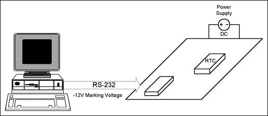
Figure 9. System connected to a PC using RS-232.
Data also corrupt when VCC falls too fast, which can either cause all the time, date, and RAM data, or only one or two bytes of data to corrupt. This second issue (one or two bytes of corrupted data) normally affects parallel-interface RTCs, e.g., timekeeping RAMs, but can also affect multiplexed-bus RTCs, as explained below.
The power-fail circuitry on battery-backed RTCs usually includes some filtering to ensure that a momentary glitch on VCC does not cause an inadvertent write protect. The write can occur if VCC falls too fast. As VCC falls, the output voltage-high level from the microprocessor's CE, OE, and WE outputs (or other control signals) usually tracks VCC. Therefore, the RTC's CE, OE, and WE inputs also follow VCC. As with typical static RAMs, if CE, OE, and WE are all low, the RTC is in a write cycle. If the RTC does not enter power-fail before VCC reaches the input thresholds of the control inputs, the RTC's internal logic will cause a write to occur.
In the case of multiplexed-bus clocks, the address information is latched on the falling edge of ALE. If R/W and CS go low before the part is in write protect, the data in the last register accessed will be corrupted. One should verify that the VCC rise and fall times meet the data sheet requirements. If the seconds register is corrupted, the RTC may appear to lose time in battery backup. The seconds register can be written to zero when corrupted. Consequently, when VCC is again applied, the resulting time will be slow by however many seconds the register was at when VCC was removed.
If all the data is corrupted, then VCC fell too fast for the RTC to switch over to the backup supply and maintain the time and date information. This problem can affect both serial-interface and parallel-interface RTCs.
Intermittent Data Loss
Intermittent data problems have been caused by interrupts routines that are not handled correctly. In some cases, the time and date information is copied to RAM, and the copies are not kept in sync. Additionally, in-circuit emulator (ICE) hardware can be configured improperly, causing erratic behavior.
Oscillator Problems
The most common reason for the clock not to increment is that the oscillator has not been enabled. Most Dallas Semiconductor clocks have a bit, usually located in the seconds register, that must be set before the oscillator will run.
The oscillator circuit is designed to be low power to prolong battery life. Problems with the crystal connection can reduce the loop gain, preventing the oscillator from running. External capacitors or other components connected to the crystal will also reduce the loop gain, increase the startup time, or prevent oscillation. Crystals with an ESR above the recommended maximum value will also decrease the loop gain. Some water-wash solder fluxes can appear to leave the PCB clean, while leaving enough contaminates to prevent oscillation. See application note 58, Crystal Considerations for Dallas Real-Time Clocks for more information.
SPI is a trademark of Motorola, Inc.