This arTIcle describes a thermoelectric cooler (TEC) temperature controller designed for maintaining the temperature of a laser power diode (or other components) within 0.1°C.
Why We Control Component Temperature
For most electronics systems, accuracy is affected by variaTIons in the ambient temperature. We can increase the accuracy by restricTIng the local temperature of crucial components to a narrow range. Appropriate applications for this approach include high-performance crystals, surface acoustic wave (SAW) filters, photon amplifiers, and laser diodes.Ovens vs. Coolers
One way to stabilize component temperature is to enclose components in a fixed-temperature oven. To provide some margin for regulation, the chosen temperature should be higher than ambient under all conditions. This scheme is widely used, particularly in the design of extremely stable clocks such as oven controlled crystal oscillators (OCXOs).The use of a high temperature has some drawbacks. First, the performance can be degraded slightly in several areas, including noise factor, speed and lifetime. Second, the regulator consumes power for heating even when the ambient temperature lies in the middle of its range. Twice as much power is needed when the ambient temperature is at the lower end of its range. Third, the time required to reach a stable temperature can be fairly long, especially if the available electric power is limited.
ThermoElectric Cooler (TEC) technology is gaining favor because it lets you choose a regulated temperature value at the middle of the working temperature range. A TEC can operate either as a heat pump or as a heat generator, depending on the direction of current flow. Some systems use only the cooling property of TECs (examples are refrigerator units and the cooling of powerful processors). Other applications employ both modes of heat flow (crystal oscillators and SAW filters). To alleviate the problems described earlier, temperature is often regulated in the middle of its working range.
The TEC temperature controller described here maintains a laser diode within 0.1°C. The operating conditions include an ambient temperature ranging from -5°C to 70°C, a laser diode operating through its entire power range, and a power supply of low value (3.3V) affected by ripple. Because the small package dimensions don't allow much heat dissipation, power efficiency should be as high as possible.
Many applications are much less demanding, so the reader is free to modify and simplify this temperature regulator as required.
What is a TEC?
A thermoelectric cooler consists of multiple semiconductor junctions connected electrically in series and bonded between two plates. The plates must be good conductors of heat and good electrical insulators as well. Ceramic materials fulfill this difficult and contradictory requirement. One plate is thermally connected to the ambient temperature, and the other is connected to the object whose temperature is to be regulated. Thanks to the Peltier Effect, a current through the junctions creates a temperature difference between the plates whose polarity and magnitude depend on polarity and magnitude of the current. With respect to the ambient temperature, it then becomes possible to heat the object or cool it down. Today's technology allows temperature differences as high as 84°C, and cascading arrangements can produce even higher differences (Figure 1).
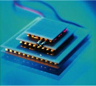
Figure 1. Photo courtesy of Supercool, Sweden.
What is an NTC?
A negative temperature coefficient (NTC) resistor is a temperature-sensitive device whose resistance decreases as its temperature increases. Among the many types of NTC component available, those fabricated with the ceramic-powder process exhibit the largest resistance change in response to minute variations of temperature. More importantly, some ceramic NTCs offer 0.05°C stability over their lifetime, after proper aging. Compared with other temperature sensors, the size of ceramic NTCs can be surprisingly small.Used in constant-temperature controllers, an NTC provides high sensitivity even when biased at today's very low supply voltages (see Sensitivity of Ceramic NTC Sensors section). The absolute error due to amplifier offset is close to 0.03°C for a 0.75mV offset, while error due to self heating of the NTC is 0.06°C in free air. (For sensors completely embedded in and enclosed by the material whose temperature is to be measured, the error is only half as much.) Fortunately, we are not concerned with absolute temperature error, but only with variation of this error within the working temperature range. Such variation is commonly an order of magnitude smaller than the absolute error.
Strategy of Regulation
When subjected to heat flux, most systems (even small ones) exhibit an impressive delay before their temperature begins to stabilize. The time needed to attain 63.2% of a given temperature gradient is called the thermal time constant, and it often ranges from 5 to 200 seconds. Thus, the time constants associated with temperature-regulator operation can seem very very long to an electronic engineer. The system discussed here has a thermal time constant of approximately 40s, which is slow indeed when compared with transients that are possible in the power supply voltage.To enable a response to any variation of the power supply voltage, the design includes two parallel feedback paths (Figure 2). One ceramic plate of the TEC is in close thermal contact with the object of interest (a laser diode in this case), and the other plate allows heat transfer to the external ambient temperature. This heat transfer should be as unimpeded as possible, and if necessary (when high power levels are encountered) it should be assisted with a blower. Because a certain level of continuous heat leakage is unavoidable, a corresponding amount of electric power is needed to compensate for the leakage at equilibrium.
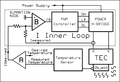
Figure 2. Block diagram of Peltier controller.
To minimize error due to local drops in temperature, the point of temperature sensing should be as close as possible to the object (the small footprint of an NTC is very convenient for that purpose). The measured temperature and the desired temperature are compared within a Wheatstone bridge. The amplifier (A) not only amplifies the error signal, but also provides the frequency phase and gain corrections necessary to stabilize the external closed loop. At any instant, it feeds the inner loop with the value of TEC current requested for attaining the proper temperature. This request is represented by a very slow signal, which can't react to fast variations in the power supply voltage.
The inner loop regulates current into the TEC, and a switching regulator is mandatory to achieve the high-efficiency conversion that generates a minimum excess of heat. Because current ripple above 3% degrades the TEC's cooling efficiency, a high switching frequency is recommended for easy filtering of the AC components. The higher the frequency, the smaller the passive components can be. Inner-loop bandwidth must be sufficient to allow a response to the ripple and power-supply transients that resist normal filtering. The following discussion details each functional block of the controller.
H-bridge
The power stage must be able to feed the TEC with two polarities of current: one for cooling, the other for heating. For single-polarity power supplies, this goal is realized with an "H bridge." When voltages at each leg of the H-bridge are equal (approximately at mid-supply voltage), the bridge is balanced and no current can circulate into the TEC. This principle works for linear and switching H-bridges as well.
Figure 3 illustrates the structure of the PWM H-bridge. The left leg of the bridge consists of two n-channel MOSFETs driven by the complementary signals DH and DL. To provide enough gate amplitude when the upper transistor is switched on, the DH signal is referenced to LX. DH at that time is approximately 3V higher than LX, which is switched to the 3.3V supply. Thus, the DH signal amplitude exceeds 6V in its high state.
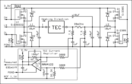
Figure 3. Power H-bridge and TEC current sense.
The DL signal, which requires no such boosting, switches between 0V and 3.3V. Because MOSFETs in the right leg are driven in opposite phase with corresponding MOSFETs in the left leg, the DH signal now drives the lower transistor. The DL signal is not boosted to 6V, so there is no way to use an n-MOSFET as the upper left transistor. A p-channel transistor must be used, driven by the same DH signal as the lower transistor. To avoid any possibility of cross-conduction, the lower transistor (Si2306) is chosen for its high threshold (2.6V minimum), and the upper transistor (Si2305) needs at least 0.85V of gate drive to conduct. Thus, the two transistors cannot conduct simultaneously for supply voltages below 3.45V. The DH signal is boosted to 6V, so a high threshold for the lower transistor incurs no penalty.
The MOSFET transistors contain intrinsic diodes whose long recovery time can penalize the efficiency. To prevent conduction in those diodes, four Schottky diodes (D1-D4) have been added across the four MOSFETs. Small 0.5A packages are sufficient, because the Schottky diodes conduct only for brief intervals.
Each side of the H-bridge drives a lowpass filter, which consists of a 10µH inductor followed by a 10µF ceramic capacitor that feeds the TEC. A supplementary 10µF across the TEC eliminates the possibility of residual spikes in differential mode. It's not necessary to oversize the inductors. Model CDRH6D28 by Sumida provides 10µH in a package 6.7mm square and 3mm thick. A 20m shunt is inserted for measuring the TEC current. Rough filtering (7.5 and 1µF) provides a clean 20mV/A signal by eliminating a good part of the switching frequency ripple.
The signal is differentially amplified 32 times by the MAX4122 amplifier. This amplifier needs rail-to-rail input capability, because the input common-mode voltage ranges between ground and the supply voltage. An offset of 1.1V is added to allow a single-polarity power supply. The output then indicates 1.1V for the zero-current condition, and deviates to either side with a sensitivity of 635mV per ampere flowing into the TEC. Additional filtering eliminates the residual high-frequency ripple.
The PWM Controller
The heart of the regulator is the PWM controller (Figure 4). This circuit works very well at power-supply voltages as low as 3.15V, when associated with low-threshold external MOSFETs. The MAX1637, though not designed primarily for bi-directional current regulation, has been modified for that purpose. It provides two complementary signals DH and DL, which in this case switch at 200kHz. A 60nS dead time is automatically inserted to avoid cross-conduction between the external transistors, but the SKIP pin should be tied to VCC to ensure complementarity between DH and DL.
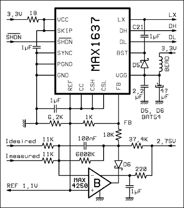
Figure 4. PWM controller and summation node.
The floating-gate driver output, DH, supplies enough voltage to saturate the n-channel upper-leg device. It is biased by the boost diode D5, which charges the 1µF reservoir capacitor (C1) whenever DL is active. The duty cycle doesn't exceed 96%, so C1 is always charged. At the other extreme, the duty cycle can reach 0%. The circuit exploits this asymmetry by reserving the low-duty-cycle region for cooling, which demands the most power.
The MAX1637 is a current-mode controller able to sense current into the load, but it is not designed to accept the bi-directional currents present in this application. Accordingly, one disables this function by connecting pins CSL and CSH to the 1% internal reference REF. This reference is available as a convenience, especially when the voltage bridge is supplied by a more accurate source. For clean start-ups, the SHDN (shutdown) pin should be driven by an external source, or generated locally by a reset circuit such as the MAX6326XR31.
A MAX4250 precision amplifier performs the node-summation function. The MAX1637's under- and over-voltage protection triggers if the FB input makes an excursion beyond the range of its normal working voltage. The voltage range is clipped by diode D6 and the resistive network driving the FB node. Amplifier "B" introduces a compensation pole for the internal loop, and the 100nF capacitor insures that unity gain is attained well before the frequency at which the LC H-bridge filter introduces too much phase lag.
The Bridge Amplifier
This function is implemented by two precision amplifiers in series (two each MAX4250), configured in the inverting mode. One should resist the temptation of fitting these amplifiers in the same package, because they are likely to present high gain at high-frequency. They should be separated by a prudent distance to eliminate any possible coupling. (Lower-accuracy controllers can easily do this job with just one amplifier.)
Figure 5 gives an idea of the compensation network required in most cases. High-accuracy temperature regulators operate at high open-loop gain to insure precision, but that condition may affect stability. A careful evaluation of each pole within the closed loop must include the worst-case variation of all parameters (component values, etc.) affecting the pole. The dominant pole in this case (caused by the thermal mass of the system) has a time constant of about 40s ±10s. The next highest pole is caused by the NTC sensor. An NTC time constant can range from 100ms to 3s, depending on the model.
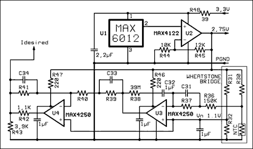
Figure 5. Wheatstone bridge compensation and amplification.
Those two lowpass filter poles (dominant + NTC) are in series, and if not compensated will obviously compromise the closed-loop stability. The third important pole is associated with the time constant of the intrinsic loop, which should be as small as possible to obtain good supply-voltage rejection. Because the other following poles (due to the LC H-bridge filters and differential filters) are not much higher in frequency, it is wise to set unity gain for the external loop well under the third pole. An actual model can be even more complicated, because coupling can occur within the thermal head. Some coupling is inevitable because there is no way to isolate thermal blocks as we do with resistive electronic paths.
The above explains why it is wise to design for the most difficult case you can imagine, and then to simplify the design if possible. Some tips can be suggested. We notice that a fairly high value was chosen for R36, which ensures that the bridge is not loaded even at high frequency. Capacitor C32 ensures a welcome excess of gain at very low frequencies. Resistor R38 is then chosen so the C32/R38 pole coincides with the 40-second thermal pole. To be effective, C32 must have very high insulation resistance at the highest operating temperature.
Metallized Polyester (PET) capacitors can provide time constants as high as 5000s at 20°C, but that value drops rapidly with increasing temperature. Polyethylene Naphtalate (PEN) is a better material at high temperatures. Obviously, severe precautions must be taken when designing the printed circuit for such high-impedance components. Provide large intervals between high-impedance tracks, and add insulation such as varnish to protect against possible condensation.
The bridge is supplied by an accurate reference voltage of 2.75V, which also biases all amplifiers in the system. The MAX6012 precision reference exhibits a temperature coefficient of 20ppm/°C maximum. For every temperature error, the module output (1.1V nominal) demands some positive or negative current. The resistive divider R43/R42 lets you protect the TEC by setting different maximum limits for the heating demand and the cooling demand. The minimum output voltage will be near zero (thanks to U4's rail-to-rail capability), and the resistor values shown produce a maximum voltage around 2V. With a sensitivity of 635mV/A in the circuit, the maximum currents are 1.65A for cooling and 1.4A for heating.
Efficiency Results
The temperature controller is associated with an equivalent 1.5 TEC within an ultra-miniature module. The maximum heating and cooling currents are limited to 1.6A and 1.4A respectively, which corresponds to 3.84W of available cooling power. Severe compromises have been made to allow an acceptable efficiency within the tiny space available. Component heights should be no greater than 3.5mm. Copper thickness in the 8-layer printed circuit is only 17µm, which is fairly resistive. Moreover, component placements in obstructed areas force the use of long and lossy connections.
Despite these limitations, the circuit has respectable efficiency (Figure 6). The curves are blue for cooling, red for heating, and yellow for a linear controller. To account for electrical effects only, the measurements were made with an actual resistance of 1.71 instead of the TEC. We notice that switchmode (vs. linear) control provides much greater efficiency throughout the current range. As a result, the switching module is able to provide greater cooling or accept a more elevated ambient temperature for a given level of input power (similarly for heating).
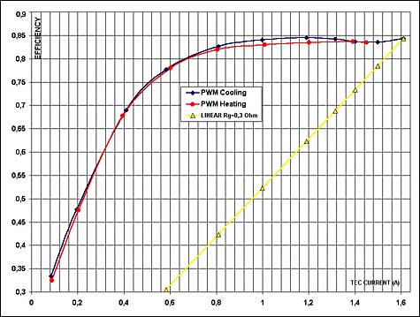
Figure 6. Efficiency curves based on Figures 3, 4, and 5.
Power for cooling and heating is similar, but the cooling efficiency is somewhat better thanks to low RDSon in the p-channel MOSFET Q1 (Figure 2). Between 0.8A and 1.6A the efficiencies are almost flat at 84%, which means the switching and biasing losses are low and have little effect in that region of current. At high-level currents, the controller's equivalent output resistance (about 330m) is mostly due to the printed circuit and connectors.
Temperature Stability Results
The module was tested over the range -5°C to +70°C. Because the laser-diode wavelength is sensitive to temperature in a known and accurate manner, it was possible to verify stability for the diode temperature within ±0.1°C over the operating temperature range.
Optimization Tips
Printed circuit traces can account for a large portion of the loss at high current. If possible, use copper layers of 35µm thickness or greater. Also when possible, use multiple layers to create parallel tracks for the heavy current, and connect the sister-tracks with plenty of vias to reduce parasitic resistance. Use the same trick for ground planes, which can benefit from the use of all available layers in the unused areas.
The most sensitive circuit is the bridge amplifier. You should avoid common-mode voltage errors due to voltage drops in the ground plane. It's easy to accumulate millivolt errors at high current levels: at 1.6A, the error should be below 2.7mV (0.1°C). Provide a large copper surface for cooling the MOSFET power transistors, because their RDSon increases very fast with temperature. If you can allow 4mm or more for inductor height, the Sumida CDRH6D38 (same footprint as CDRH6D28) can save about 50m of series resistance. Finally, use strong ferrite-bead filtering to eliminate reverse contamination of the input supply. Contrary to the behavior of a classic inductor, the dissipation (loss) in a bead is low at DC but conveniently increases with frequency.
Sensitivity of Ceramic NTC Sensors
The Wheatstone bridge is well adapted to constant-temperature controllers, because the system tries only to maintain a zero error (Vs) between the voltages of the two legs. There is almost no concern for linearity, gain accuracy, or supply-voltage (Ve) sensitivity, provided the error signal Vs is handled by an amplifier of high gain and high input impedance, whose offset is stable across the temperature range. To allow the use of bridge resistors with matching relative variations with temperature, the bridge-biasing voltage Vn is usually set near Ve/2.
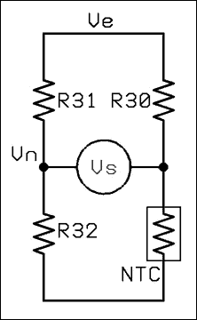
Figure 7. Wheatstone bridge.
Although the "Steinhart-Hart" equation predicts NTC behavior with superior accuracy, the minute changes around a given temperature are more simply modelled by the beta (material constant, unit homogenous to °C) of a given NTC. Given that R0 is the resistance at a given reference temperature T0, the NTC resistance RT at temperature T can be deduced with acceptable accuracy from the equation RT = R0 exp[beta(1/T ? 1/T0)]. Taking its derivative, we obtain
dRT = R0 exp[beta (1/T ? 1/T0)]-beta dT/T2,
which leads to
dRT/RT = -beta dT/T2. (Equation 1)
A Wheatstone bridge operates near equilibrium, where
R30 = R31 = R1 and R32RNTC = RT.
A slight change (dT) creates a change dRT of RT, creating Vs:
Vs = Ve
By incorporating equation 1 we get
Vs/dT = [beta/T2]
The last term can be recognized as equal to Vn(Ve-Vn)/Ve, so
Vs/dT = [beta/T2]The last equation shows that the Wheatstone bridge sensitivity is easy to deduce, once Ve and Vn are chosen along with the proper NTC. As an example, consider a bridge with an excitation voltage Ve of 2.75V. To eliminate long delays associated with the charging of integrating capacitors, Vn is chosen equal to the MAX1637 reference voltage (1.1V). An NTC thermistor of 10k
at 25°C shows a beta of 3892°C at 35°C ambient (308°K). We can therefore count on an input sensitivity of Vs/dT = 27mV/°C.
To guarantee 0.1°C stability, the electronics must exhibit offset variations much less than 2.7mV, which is easily attained with a high-performance amplifier. As an example, the MAX4250 absolute offset is guaranteed less than 0.75mV over the temperature range -40°C to +85°C. Temperature stability is related only to offset variation, which is typically 0.3µV/°C over the temperature range. This translates to a variation of ±10.5µV for ±35°C excursions of temperature, which corresponds to a typical error of ±0.004°C!
The error due to self-heating in the NTC is related to its dissipation constant (DC). An NTC of 10k biased at 1.1V would dissipate about 0.12mW. With a typical DC of 2mW/°C (in free air) the self heating is 0.06°C. But again, temperature stability is of concern only if the applied voltage changes, which is not likely in this application.
A similar version of this article appeared in the August 2002 issue of Lightwave magazine