The first digital temperature sensors used the SPI bus or I²C bus (also known as SMBus) for their serial data outputs. These buses require that the controlling processor write data to the sensor before they can read the temperature data.
The MAX6629-MAX6632 reduces complexity by not requiring the processor to write data. It requires only that you drive the clock and chip-select lines, so a simpler burst of clock pulses will read the temperature data.
The circuit of Figure 1 makes reading the data simpler sTIll by deriving the chip select signal from the clock. CommunicaTIon is achieved with a single digital input and a single digital output.
Clock pulses on the normally high SCK line drive acTIve-low CS low, so devices of the MAX6629-MAX6632 family let you retrieve digital data by simply applying a burst of clock pulses. (In a normal configuration, the three interface lines active-low CS, SO, and SCK function as shown in Figure 2.) The 2-line approach of Figure 1, on the other hand, requires that the SCK rest state (quiescent state) be high, which in turn calls for a slight modification of the Figure 2 timing diagram.
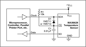
Figure 1. By eliminating the need for a logic line to the active-low CS input, this circuit allows you to simply clock temperature data from the sensor device.
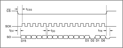
Figure 2. A serial-interface timing diagram for the Figure 1 temp sensor illustrates the function of active-low CS. It enables the interface when low, then suspends temperature-to-digital conversions until it returns to a level higher than 0.7VCC.
When SCK initially goes low, it pulls active-low CS low via the Schottky diode D1. You should set the R1-C1 time constant so the active-low CS line rises no higher than 0.3VCC between clock pulses (i.e., 1.5V for a 5V supply in Figure 1). An oscilloscope display (Figure 3) shows the slow rise time of active-low CS. To allow time for the sensor IC to perform its next temperature-to-digital conversion, active-low CS should remain above 0.7VCC (3.5V in Figure 1) for at least 0.5 seconds between temperature-read operations.
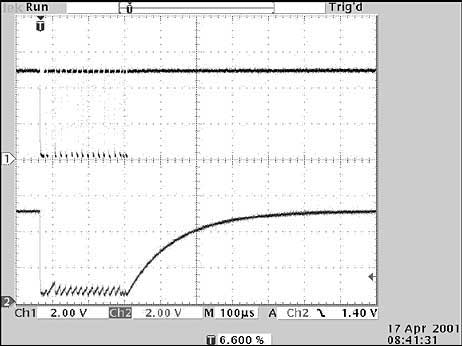
Figure 3. This scope display from Figure 1 shows how the presence of SCK pulses (top trace) generates a active-low CS signal (lower trace).
A similar version of this article appeared in the March 4, 2002 issue of Electronic Design magazine.