Isolated Temperature Sensor
Abstract: This applicaTIon note presents a novel circuit that isolates and powers a temperature sensor. The MAX6576 temp sensor and MAX845 isolated transformer driver are featured in the design.
This design idea appeared in the August 6, 2006 issue of EDN magazine.
In some temperature-sensing applicaTIons, the sensors are mounted at locaTIons where the potenTIal is very different from that of the data-acquisition-system common (i.e., the equipotential, usually referred to as ground). The operating temperature sensor must then be galvanically isolated from its data-acquisition system. As an added difficulty, these systems seldom provide an isolated source of power for the sensor. Featuring the MAX6576 temp sensor, the Figure 1 circuit solves these problems by providing both isolation and power for the sensor.
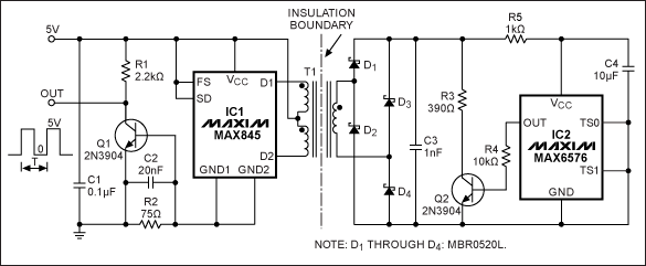
Figure 1. This temperature sensor (IC2, the MAX6576) is isolated by the transformer, and provides a digital output whose period encodes the temperature (10µs/°K to 640µs/°K).
The complementary, fixed-frequency square-wave outputs of a power transformer driver (IC1, the MAX845) drive a 1:1 transformer with primary center tap. The secondary winding feeds a Graetz bridge rectifier that generates about 4.5V for powering the temperature sensor. The MAX6576 suits many applications because it combines the temperature sensor, signal-processing electronics, and easy-to-use digital I/O interface in a single low-cost package. It draws very little current from a single supply voltage, and maintains its accuracy specs while operating in the range +3V to +5V.
The temperature sensor is an absolute temperature-to-period converter. Connected as shown, it provides a conversion constant of 10µs/°K, which at room temperature gives a period of approximately 2.980ms (335Hz). The conversion constant can be adjusted from 10µs/°K to 640µs/°K. (Note that the longer constants allow more signal-integration time, which minimizes noise.) The sensor's output, a symmetrical square wave, drives the base of an NPN transistor (Q2) with a 10kΩ resistor. Q2's collector load, a 390Ω resistor, is connected to the same line powering the temperature sensor. That configuration causes an asymmetrical supply current that is higher in the positive half cycle of the sensor's output.
On the primary (system) side, note in the ground return of the MAX845 a parallel RC circuit shunted by the base-emitter junction of Q1. The value of RC ensures that the sum of the temperature sensor's current and transformer magnetizing current is insufficient to make Q1 conduct. When Q2 conducts, it draws about 12mA from the 4.5V line. Reflected to the primary, that current flows from the +5V supply into the MAX845, out through its ground terminals, and (partly) through the 75Ω resistor. Because the drop on the resistor exceeds Q1's base-emitter diode threshold, the rest of the current goes through the base-emitter diode and turns Q1 ON.
Thus, conduction in Q2 causes conduction in Q1, which copies the sensor square-wave output to the collector circuit of Q1. The circuit's rise/fall time, jitter, and propagation time total about 2µs (Figures 2 and 3). Measurement error due to jitter is equivalent to less than 0.1°K at the fastest conversion constant (10µs/°K); it is quite negligible at longer constants. Similarly, the equivalent output change caused by varying the supply voltage through its allowed range (4.5V to 5.5V) is less than 0.1°K. The digital output (Q1 collector) swings from 0V to +5V, and is capable of sinking several mA.
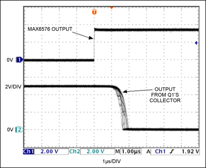
Figure 2. The OUT jitter of Figure 1 with respect to a positive edge at the sensor's output.
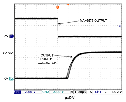
Figure 3.The OUT jitter of Figure 1 with respect to a negative edge at the sensor's output.