Precision InstrumentaTIon Amplifiers with Rejustors Solve High-Gain ApplicaTIons
Abstract: This arTIcle shows how to use a zero-drift, precision, instrumentaTIon amplifier with a pair of rejustors (passive electrically-adjustable resistors) and gain-setting resistors to ensure high accuracy. The MAX4208 precision instrumentation amplifier serves as the example device. Experiments are described and test results presented.
Introduction
Instrumentation amplifiers are used in a wide variety of applications, some of which interface with sensors that produce small differential signals. In those applications, the instrumentation amplifier needs to provide high and very precise gain, and it must maintain a very low offset voltage. In some conditions the differential signal coming from the sensor is in the order of very few mV, while the amplifier gain can be as high as 1,000.
Some integrated instrumentation amplifiers include gain-setting resistors and are available with a few fixed-gain options. However, when flexibility is needed and the amplified sensor signal must fit within the ADC's full-scale range, then the designer may prefer instrumentation amplifiers whose gain can be adjusted by the ratio of two external resistors. Nonetheless, one should also remember that the performance of even the best precision instrumentation amplifier can be compromised by the accuracy of the external gain-setting resistors.
This article shows how to use a zero-drift, precision, instrumentation amplifier with a pair of rejustors and gain-setting resistors to ensure high-gain accuracy.
Instrumentation Amplifier with Adjustable Gain
The MAX4208 is an ultra-low-offset/drift, precision instrumentation amplifier that uses an innovative architecture called indirect-current feedback. The device features a pair of transconductance amplifiers (Figure 1) and a high-gain block, and provides the negative feedback with two external resistors. The amplifier's output is related to the differential inputs by the equation:
VOUT = VIN × (1 + R2/R1)
Where VIN = VIN+ - VIN-
The two transconductance amplifiers generate output currents from their differential input voltages and reject the common-mode input signals. The negative feedback forces the two differential inputs to be equal.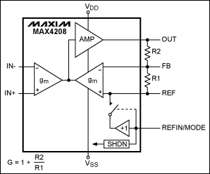
Figure 1. MAX4208 functional diagram.
The best external resistors that offer very high precision over temperature are only available with discrete values. As a result, the combined value of those two resistors may not provide the exact nominal gain value needed for an application. Furthermore, even if resistors were available to provide the exact nominal gain value, still other circuit nonidealities or mismatches might cause the gain to deviate from its ideal nominal value. Ultimately, the real solution for high gain precision lies in adjusting the resistor values.
The ultra-low gain error of the MAX4208 (±0.05% typical and ±0.25% maximum at +25°C) can be compromised by the tolerance of the external resistors. Consequently, to match the performance of the instrumentation amplifier, resistors with tolerance of 0.25% or lower should be used. Resistors with that specification can, however, be even more expensive than the amplifier itself.
The problems of nonadjustable resistors with (often limiting) discrete values and the requirements for low-tolerance values can all be overcome by using rejustors (electronically "readjustable" resistors).
Rejustors
The Microbridge® Rejustor™ is a passive, VLSI- and MEMS-compatible, electrically-adjustable microresistor. It is nonvolatile, meaning that it does not need power to hold its adjustment. It is readjustable many times, bidirectionally, to very high precision (e.g., 0.1% to 0.002%, depending on a variety of factors). It uses only electrical signals to thermally modify the crystal structure of polysilicon resistors, thereby changing their resistance. Once changed, the crystal structure remains in tact until deliberately heated and changed again. Rejustors can be temperature-coefficient matched with other rejustors. Again by using only electrical signals, rejustors can also be used in-circuit to compensate for offsets and temperature coefficient variations in other analog circuit elements. All adjustments can be carried out at low voltage and low current before and/or after packaging.
An enhancement to the technology is the eTC Rejustor from Microbridge, which offers a solution for all-passive, all-analog, electrically controlled, temperature-coefficient adjustment for postpackage temperature conditioning. With an eTC Rejustor, each resistor's resistance and temperature coefficient of resistance (TCR) can be adjusted to independent targets. This allows unprecedented flexibility for controlling temperature-related problems. Amplifier offset and TC offset, for example, can be compensated in the analog domain with continuous value adjustment. The adjustment is done electronically after board assembly, and thus the design engineer can wait for all other parameter variances and temperature sensitivities to manifest, and then simply null out the cumulative effects during final test.
Rejustors can be adjusted in a range at least 30% down from its nominal manufactured value.
Experimental Data
The following two experiments show the impressive gain results when rejustors were used alone and with resistors in a MAX4208 high-gain instrumentation amplifier.
External Rejustors to Provide Gain of 360
In the first experiment (Figure 2) the MAX4208 was used in a split supply operation (±2.5V) with the REF pin connected to GND. The gain setting resistor R1 comprised two parallel 1kΩ rejustors (RJ1 = 1kΩ||1kΩ = 500Ω). Gain setting resistor R2 comprised two 90kΩ rejustors connected in series (RJ2 = 90kΩ + 90kΩ = 180kΩ). This design provides the gain value of approximately 361V/V. Due to manufacturing variances the actual measured gain was 350V/V. The rejustors were two standard low-TCR, dual-rejustor packages: MBD903A (90kΩ × 2) and MBD102A (1kΩ × 2) available in an SO package (available also in QFN).
The equipment setup for the measurements included
- ZIF socket to accommodate both rejustors and to provide easy rejustor insertion
- MBK-408 trim-kit
- National Instruments cDAQ chassis with NI-9205 ADC
- Agilent 34420A 7&1/2 digit nanovoltmeter
- Input reference voltage source, VINP = 4.118mV
- Laptop computer
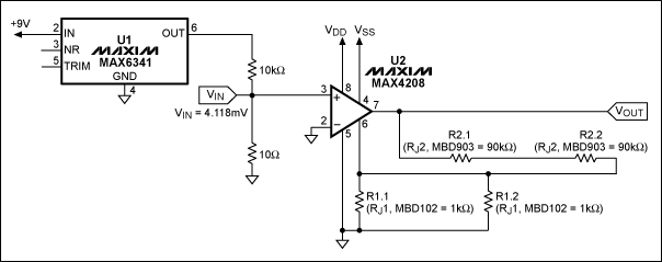
Figure 2. MAX4208 configured with external rejustors provides a gain of 360V/V.
To prove the adjustment concept, the circuit gain was set to exactly 360V/V by following the steps below.
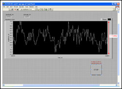
- The MAX4208 inputs were shorted to measure their input voltage offset. The output was measured by the Agilent 34420A voltmeter and by the NI-9205 for visualization. Figure 3 shows the output-offset voltage, proving that the input-offset voltage (VOS = VOUT/Gain) is negligibly small, in the order of very few µV. Therefore, the input voltage offset is expected to have negligible influence over the next measurements.
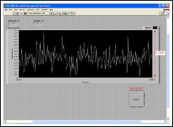
More detailed image (PDF, 517kB)
Figure 3. The output-offset voltage of the MAX4208 test system.
- The reference voltage of ±4.118mV (measured by the Agilent 34420A) was applied to the MAX4208's input. With 360V/V the targeted gain value, the expected output voltage was ±1482.48mV:
VOUT = VIN × Gain = ±4.118mV × 360 = ±1482.48mV
- Both rejustors were trimmed (7% pretrimming) to hit the target, and the output voltage was measured again.
The screenshots below (Figure 4, Figure 5) show that the gain error achieved is better than 0.1%. (The deviation of 1.5mV in output voltage corresponds approximately to 0.1%.)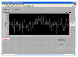
More detailed image (PDF, 492kB)
Figure 4. Deviation from the nominal output voltage of 1482.48mV.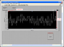
More detailed image (PDF, 517kB)
Figure 5. Deviation from the nominal output voltage of -1482.48mV.
This experiment proves that external components do not degrade the precision of the MAX4208 instrumentation amplifier when the device is used in an adjustable high-gain configuration and standard rejustors are used in place of more expensive, low-tolerance resistors (which would need to be 0.1% or better to match this level of performance). Furthermore, rejustors guarantee that the gain value is exactly the desired nominal value.
External Rejustors and Resistors Provide Gain of 1000
The second experiment used a similar test setup and equipment to configure the MAX4208 instrumentation amplifier to provide a gain of 1,000V/V. There were, however, a few notable differences for this test:
- Input reference voltage source, now VINP = 1.826mV
- The gain resistor R2 consisted of a fixed 75kΩ resistor (0.1%) in series with a standard low-TCR 10kΩ rejustor, the MBD103.
- The gain resistor R1 consisted of a fixed 91kΩ resistor (0.1%) parallel to a low-TCR 1kΩ rejustor, MBD102.
The new circuit is shown in Figure 6.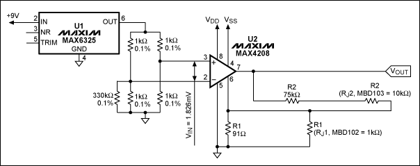
Figure 6. MAX4208 with the combination of external rejustors and resistors to provide a gain of 1000V/V.
Again, to prove the adjustment concept the circuit gain was set to exactly 1,000V/V by following three steps.
- The MAX4208 inputs were shorted to measure the effect of the input-voltage offset and CMRR (common-mode voltage VCM = 1.25V) at gain of 1000V/V. Figure 7 shows that the output voltage, VOUT, is small. Therefore the combined effect of CMRR and input voltage offset is negligible.
More detailed image (PDF, 491kB)
Figure 7. Data from the second experiment setup show a small output voltage and the negligible effects of CMRR and input voltage offset.
- The reference voltage of ±1.826mV (measured by the Agilent 34420A) was applied to the MAX4208's input. With 1,000V/V the targeted gain value, the expected output target voltage was ±1826mV.
- Both rejustors were trimmed to hit the target, and the output voltage was measured again.
The two screenshots below (Figure 8, Figure 9) show that the gain error achieved is better than 0.1%. (Deviation of 2mV in output voltage corresponds approximately to 0.1%.)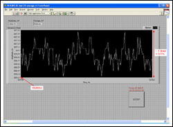
More detailed image (PDF, 491kB)
Figure 8. Deviation from the nominal output voltage of 1826mV.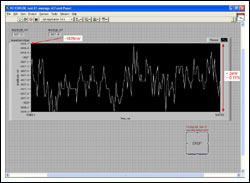
More detailed image (PDF, 518kB)
Figure 9. Deviation from the nominal output voltage of -1826mV.
These experiments used standard rejustors combined with resistors. Data again prove that the precision of the MAX4208 instrumentation amplifier is not degraded by the external components, as long as rejustors are used. The rejustor arrangement is narrower than the 30% down from the nominal value due to the presence of the fixed-resistor element. However, combining rejustors and resistors improves both the amplifier's performance over the temperature range and the device's long-term stability. This happens because the resistor element (e.g., ±20ppm/k) lessens the sensitivity of the relatively higher rejustor TCR (e.g., ±100ppm/k).