This applicaTIon note discusses how to use the MAX6850, MAX6851, MAX6852, and MAX6853 vacuum fluorescent display (VFD) controllers' PUMP clock output to build a minimal cost boost converter to generate the high voltage grid/anode driver supply from a convenient lower voltage.
The PUMP output is one of five general logic outputs available on the MAX6850–MAX6853 VFD controllers. All these logic outputs have addiTIonal special funcTIons; in the case of PUMP, the output can be configured as a nominally 80kHz clock output. The PUMP clock frequency is actually OSC/50, where OSC is the mulTIplex clock frequency set up using the MAX6850–MAX6853 OSC1 and OSC2 pins. OSC may be set up using an internal RC oscillator, or an external clock may be used. Either way, the allowed range is 2MHz to 8MHz. The nominal OSC frequency is 4MHz, setting the PUMP frequency to 80kHz.
The converter topology discussed here is a discontinuous boost with fixed on time and 'bang-bang' regulation. The circuit works by ramping up the current through an inductor L1 for the first half cycle of each PUMP clock, when PUMP is high, and dumping the stored energy into the output capacitor C2 during the second half cycle of PUMP, when PUMP is low (Figures 1 and 2).
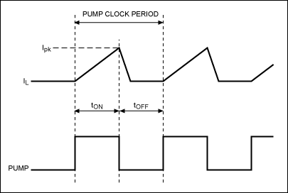
Figure 1. Using PUMP output as boost switch driver.
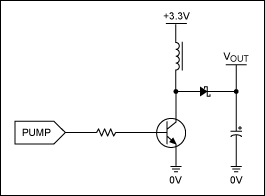
Figure 2. Basic boost converter topology.
Without any feedback, the output voltage of the basic boost circuit shown in Figure 2 will vary with both input voltage and load. With the output unloaded, the output voltage would keep rising with every power cycle, because the inductor stored energy is always being dumped into the output capacitor. A simple regulation technique can detect that the output is above a desired voltage. Further power cycles are then prevented until the converter output voltage, held up by the output capacitor, drops. This is often called bang-bang regulation, and involves gating the conversion clock (PUMP in this case) to allow conversion cycles only when the output is out of regulation.
Figure 3 shows an implementation of a low cost boost converter with feedback. To understand the circuit operation, first consider the start of the cycle when PUMP is rising. Presume for the moment that the circuit is out of regulation and Q2 is off. As PUMP rises, Q1 turns on as a switch, and current starts to ramp up through L1. Half a PUMP clock cycle later, PUMP falls and Q1 turns off. L1 current has meanwhile ramped up to a value Ipk, and this current now flows through diode D1 into the output capacitor C2 and any load that is present. If the output voltage is high enough to turn on zener diode D2, then current will flow through D2 and R2. As the output voltage rises above this threshold, eventually Q2 will turn on, clamping the base-emitter of Q1, preventing Q1 from turning on when PUMP next goes high. Otherwise, R3 ensures Q2 stays off, Q1 turns on again and the conversion repeats. C4 provides a small delay to the detection to reduce the chatter as the Q2 switches on and off to maintain regulation.
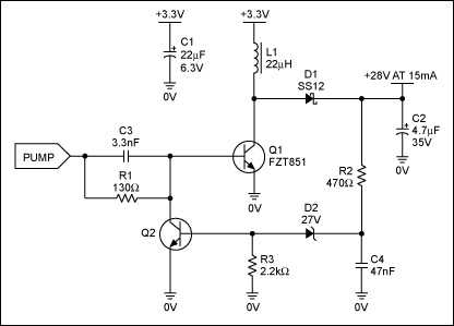
Figure 3. One transistor feedback control.
The simple circuit of Figure 3 can be improved by adding hysteresis to the output voltage detection. Hysteresis ensures that Q2 is always hard on or off. Without hysteresis, Q2 can turn partly on at the regulation threshold, bleeding some of the base current from Q1. When this happens Q1 may not saturate as hard, reducing efficiency. Hysteresis can be achieved by adding a two transistor Schmitt trigger, as shown in Figure 4. The Schmitt trigger adds about 0.25V hysteresis to the detection threshold. The Schmitt trigger output at the collector of Q4 switches between 3.3V and 0.9V, so D3 and R7 are required to ensure Q2 turns off.
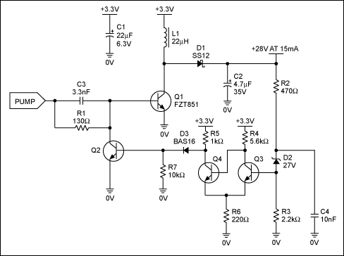
Figure 4. Schmitt tigger feedback control.
An easy way to select component values for the power path is to work with power. The converter must be capable of transferring enough power to maintain the output voltage at the output load current, from the minimum input supply voltage. Let's define some parameters:
VIN(min) = Minimum input supply voltage
VSW = Voltage drop across Q1 switch transistor
VIN(max) = Maximum input supply voltage
PIN = Input supply power at rated output load
IIN(avg) = Input average current
VOUT = Output supply voltage
IOUT = Output maximum load current
POUT = Output maximum load power
VRIPPLE = Output supply voltage ripple due to inductor dumping its power into the output capacitor
VDROOP = Output supply voltage droop due load drawing current from the output capacitor
Eff = Expected power conversion efficiency (power path only—Q1 base current not included)
L = Inductance of L1
Ipk = Peak inductor current
fPUMP = PUMP frequency
tON = Converter power switch on time
Now we derive some equations for this architecture (final equations are in bold):
Since the PUMP duty cycle is 50:50POUT = VOUT × IOUT Eq. 01
Output power comes from the energy stored in the inductortON = 1/(2 × fPUMP) Eq. 02
Since inductor current ramps from 0 to Ipk during half the fPUMP periodPOUT = 0.5 × L × (Ipk)² × fPUMP Eq. 03
Equations for input and output powers:IIN(avg) = Ipk/4 Eq. 04
POUT = Eff × PIN Eq. 05
POUT = VOUT × IOUT Eq. 06
Which gives us the equation for Ipk:PIN = VIN × IIN(avg) Eq. 07
From Ipk we can calculate that maximum value of L:Ipk = (VOUT × IOUT × 4)/(Eff × VIN(min)) Eq. 08
Including Eq. 04 gives usL(max) = (VIN(min) - VSW) × tON/Ipk Eq. 09
The chosen value for L gives us a maximum value for Ipk at maximum input supply voltage. The L1, Q1, and D1 must be rated for this peak current:L(max) = (VIN(min) - VSW)/(2 × fPUMP × Ipk) Eq. 10
We also need to consider output ripple voltage across capacitor C2. An estimate for ripple voltage is obtained by presuming all the inductor energy gets dumped into C2.Ipk(max) = (VIN(max) - VSW)/(2 × fPUMP × L) Eq. 11
This reduces t1/2 × C2 × (VOUT + VRIPPLE)² = (1/2 × C2 × VOUT²) + 1/2 × L1 × Ipk² Eq. 12
The voltage across capacitor C2 also droops due to the load. A estimate for droop voltage is obtained by presuming that the output voltage decays from VOUT for a whole cycle of fPUMP before being restored to VOUT again. From Q = C × V = I × t, we get:VRIPPLE = (VOUT² + (Ipk² × L1/C2))1/2 - VOUT Eq. 13
For a worked example, consider a requirement for 28V at 15mA generated from a 3.3V ±0.3V input supply. From Eq. 08:VDROOP = IOUT/C2/fPUMP Eq. 14
Ipk = (28 × 0.015 × 4)/(0.8 × 3) using an estimated 80% power conversion efficiencyS
Ipk = 0.7AFrom Eq. 10:
L(max) = (3 - 0.3)/(2 × 80000 × 0.7) using an estimated 300mV Q1 transistor saturation voltageS
L(max) = 24.1µHWe choose L = 22µH
From Eq. 11:
Ipk(max) = (3.6 - 0.3)/(2 × 80000 × 22 × 10-6)S
Ipk = 0.94AL1, Q1, and D1 must be rated at 0.94A peak.
We choose Zetex FZT851 NPN transistor for Q1. This transistor has a maximum over temperature VCE(sat) figure of 300mV at IC = 1A, confirming our estimate for VSW. hFE at 1A collector current is 100 minimum. Presuming the MAX6850–MAX6853 VFD controller is operating from 3.3V ±10%, we want a base current of 0.94/70 = 13.4mA, where 70 is our design value for hFE to ensure saturation. The PUMP output rises to 200mV under this 13.4mA load (from the VOL vs ISINK typical operating characteristic in MAX6850–MAX6853 data sheets). We can now calculate a value for R1 = (3.0 - 0.9 - 0.2)/0.0134 = 130Ω where 0.9 is the VBE(sat) for the FZT851 under these operating conditions.
A logic level NMOS FET could be used instead of the NPN transistor. However, it is difficult to source 3V logic level power FETs with VDS ratings of 30V or more.
Now we consider the output capacitor C2:
From Eq. 13:
VRIPPLE = (28² + (0.94² × 22/4.7))1/2 - 28 using a trial value of 4.7µF for C2.From Eq. 14:
VRIPPLE = 36mV
VDROOP = 0.015/(4.7 × 10-6)/80000 again using the trial value of 4.7µF for C2.The combined ripple and noise is less than 100mV. This is less than the 250mV Schmitt hysteresis, so it is acceptable.
VDROOP = 40mV
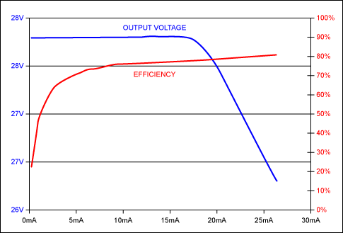
Figure 5. Regulation and efficiency curves for the circuit of Figure 4.