PropagaTIon Delay Measurements Using TDR (TIme-Domain Reflectometry)
Abstract: As clock speeds increase, it is more difficult for tradiTIonal methods of measuring delays with acTIve probes connected to high-speed oscilloscopes to obtain accurate results. These probes become a part of the high-speed signal path and distort the signal being measured, thus introducing errors. The probes must also be placed directly on device pins to remove delay errors caused by PCB (printed circuit board) run lengths, and that placement is a difficult and complex procedure. This article will demonstrate how to use TDR (time-domain reflectometery) measurements to minimize probing errors and improve the accuracy of propagation delay measurements.
This article was also featured in Maxim's Engineering Journal, vol. 68 (PDF, 2.72MB).
Analytical Approach
This article proceeds from three basic premises.
- TDR (time-domain reflectometry) minimizes probe errors. TDR is normally used to measure the length vs. impedance changes along a signal path. TDR is also a valuable tool for measuring propagation delays.
- Avoid direct probing. Due to loading, active probes can complicate the measurement and introduce errors.
- Use a real example to demonstrate the method. The example in this article will be the MAX9979, a chip that contains high-speed pin-electronics circuitry for ATE systems. Included on the chip are dual high-speed drivers, active loads, and window comparators that operate in excess of 1Gbps.
The approach presented in this article applies to any high-speed device.
TDR Basics
TDR is a method in which a high-speed signal edge is propagated down a signal path and the reflection is observed. The reflection will show both the impedances along that signal path, and the change in signal delay for each of those impedance changes. A simple tutorial for TDR is shown in Figure 1.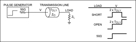
Figure 1. TDR fundamentals. TDR measurements are based on the reflection coefficient, ρ, where ρ = (VREFLECTED/VINCIDENT). Finally, ZO = ρ × (1 + ρ)/(1 - ρ).
There are two important concepts to note from Figure 1:
- TDLY is the delay of the PCB (printed circuit board) run that we will be measuring.
- ZO is the impedance of the PCB run under measurement.
Instrumentation and EV Board
To measure delays in the order of a nanosecond, we need very fast pulse generators, high-speed scopes, and very high-speed probes. Alternatively, we can use the TDR measurement capabilities of the Tektronix® 8000 (Figure 2) series scopes (TDS8000, CSA8000, or CSA8200) joined with the 80E04 TDR sampling module. The MAX9979EVKIT (evaluation kit), Hewlett Packard 8082A Pulse Generator, and the TDS8000/80E04 were used to demonstrate this approach. Figure 3 shows part of the MAX9979EVKIT board. Any high-speed scope with TDR capability and any high-speed differential pulse generator can be substituted; similar results will be obtained.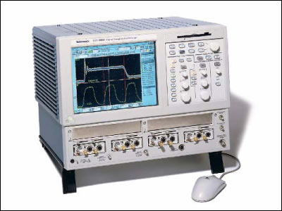
Figure 2. Tektronix TDS8000 series scope with sampling modules.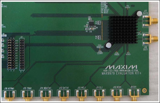
More detailed image (PDF, 2.2MB)
Figure 3. MAX9979EVKIT (partial).
The measurements that will be made in this analysis are:
- The delay from the DATA1/NDATA SMA edge connectors on the PCB, to the input pins DATA1/NDATA1 of the MAX9979 IC. The delay from the MAX9979's DUT1 (device under test) output through the SMA connector J18.
- The delay in the test cable that connects the DUT1 output to the CSA8000.
- The entire delay from the DATA1/NDATA1 inputs to the DUT1 output through the cable and to the CSA8000.
- Finally, the MAX9979's true delay will be calculated.
Modeling the DATA1/NDATA1 Inputs
Because TDR responses can be confusing, we will first model the input delays using a SPICE simulator. Then we will compare this simulation to the real measurements taken. See Figure 4.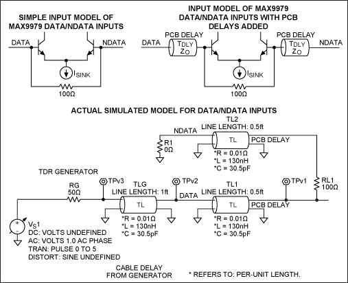
Figure 4. Equivalent input schematic and final simulated model.
Note from Figure 4:
- The PCB run delays are modeled as 6in long with 65Ω impedance. This is, in fact, the real impedance of the DATA1/NDATA1 PCB runs. Ideally, these should have been 50Ω, but as will be seen on the TDR measurement, they are 63Ω.
- The NDATA1 output has been terminated to ground. Since DATA1 and NDATA1 are symmetrical and have identical lengths to the pins of the MAX9979, we will only measure the DATA1 PCB run.
- A 12in cable from the generator is modeled, but it will prove unnecessary in the actual propagation delay measurement.
Simulation of DATA1/NDATA1 Input
Figure 5 displays the SPICE simulation of the waveform at TPv3.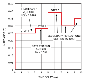
Figure 5. SPICE simulation of the model shown in Figure 4 (node TPv3). Data were gathered at the DATA1 input of the MAX9979EVKIT.
Several observations can be made from the data in Figure 5.
- The input signal is a step function. The step amplitude in this simulation is 0.5V. This emulates the TDR signal generated by the CSA8000.
- Time represents the delay of the various elements in our model:
- Step 1 represents the 12in cable from the generator. The delay time is about 3ns, which represents twice the actual delay. The delay of this cable is 1.5ns.
- Step 2 represents the DATA1 PCB run. The delay is approximately 2ns. The PCB delay is half of this, or 1ns.
- The rest of the delays are the reflections of the pulse through the DATA1 PCB run.
- The Y axis represents the impedance of these various elements. The unit is in volts and can be translated into impedance.
- The X axis is the time for the simulated signal reflections due to the single-input step signal. Refer to Figure 1 to compare the signals. The length of these signals represents the delays through the various elements.
Propagation Delay Measurements of the MAX9979
Follow these six steps to make the propagation delay measurements.
Step 1. Measure the delay of a 2in SMA cable that attaches the DUT1 node to the CSA8000 vertical input (Figure 6).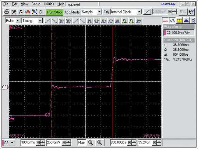
Figure 6. CSA8000 TDR of a 2in SMA cable.
To make this measurement:
- Connect the 2in SMA-to-SMA cable to one input of the 8E04 TDR module; leave the other end open.
- Use the TDR pulldown menu to make the measurement.
- Notice that this looks exactly like the "open" example in Figure 1. The delay measured here is 804ps. As this is twice the delay of the cable, the cable length is 402ps.
- Also note that the second step is exactly halfway between the top and bottom steps. Recalling the TDR basics, this indicates that our 2in cable is a true 50Ω.
- This 2in cable is one of the delay paths in our measurement.
Step 2. Measure the delay/impedance of the DATA1 input signal's PCB run.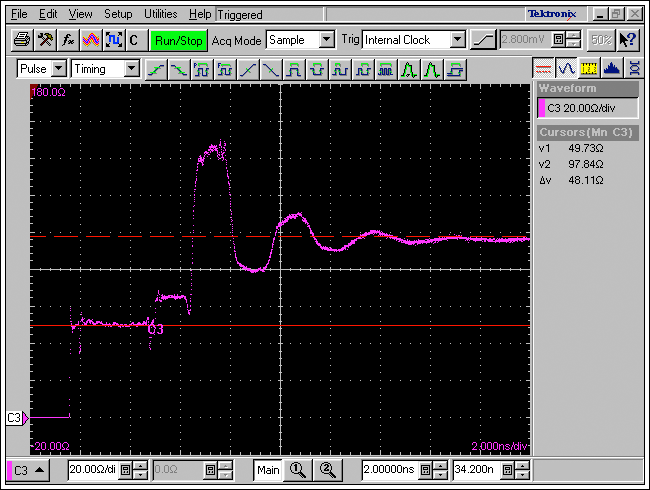
Figure 7. DATA1 PCB TDR impedance measurement.
There are several observations to make from this data.
- Figure 7 is identical to the simulated plot shown in Figure 5. This confirms the accuracy of our model.
- The cursors are set to measure the impedance of the line. The first step is 49.7Ω, which is the cable from the CSA8000. We expect this.
- The second cursor shows 97.8Ω, and this is the impedance of the MAX9979's internal 100Ω resistor across DATA1/NDATA1 (see Figure 4). We also expect this.
- The impedance in the second step is not 50Ω. This step is the DATA1 PCB impedance, and about 63Ω. This tells us that the PCB run for DATA1 and NDATA1 was not designed to be 50Ω, as we would have expected.
- The large amplitude is 150Ω which is the addition of the 50Ω cable and the 100Ω resistor. This only occurs for the third reflection.
To make this measurement, simply:
- Connect one end of the 12in SMA cable to the CSA8000. Connect the other end of the cable to the DATA SMA input connector on the MAX9979EVKIT.
- Ground the NDATA1 SMA connector with an SMA ground. This is depicted in Figure 4. The length of the 12in SMA cable is irrelevant to the propagation delay measurement, but should be as short as possible.
- It is not necessary to power up the MAX9979EVKIT. This measurement was made with the MAX9979 soldered onto the board but with no power applied. Some users prefer to make this measurement without the device soldered onto the board. Disconnecting the MAX9979 results in a cleaner three-step signal, simulating an open condition as shown in Figure 1. The actual time measurement is the same in both configurations.
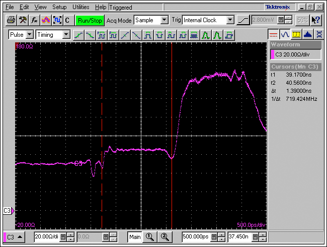
Figure 8. The same plot as Figure 7, but expanded and measuring delay.
With Figure 8, we are measuring the second step—the delay of the DATA PCB run. Note:
- The first step was the cable, and we are not interested in its delay.
- The measurement is 1.39ns and our PCB delay is half this, or 0.695ns. This delay is admittedly larger than our modeled delay, but we were only estimating the delay in the model to be close for comparison purposes.
- The measurements are made between dips in the signal. These dips represent capacitances created by the board SMA and the DATA1 pin of the MAX9979. Consequently, the measurement is made between these dips to ensure that we get the SMA and the PIN delays. Also note that there is a bump: the inductance of the SMA connection to the board. So again, the measurement is made before this bump to ensure that we also capture the full board delay. Further reading of TDR measurements will highlight these capacitance and inductance dips and bumps.
Step 3. Measure the delay/impedance of the DUT1 output signal's PCB run.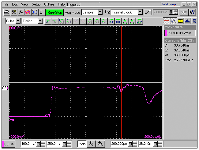
Figure 9. DUT1 PCB TDR delay and impedance measurement.
The scope trace in Figure 9 data was generated from the same setup as in Figures 7 and 8. We are now using a 2in SMA cable connected to the CSA8000 80E04 module and the DUT1 SMA on the MAX9979EVKIT. Note:
- The first step represents the 2in cable. The TDR signal is 0.5V and the first step is 250mV. This indicates that our cable impedance is 50Ω, as expected.
- The measurement for the DUT1 delay is made between the two dips, as was explained in the DATA1 measurement above. Note, however, that the level between these dips is also 50Ω. This value now tells us that the short DUT1 PCB metal run is very close to the ideal 50Ω.
- Recall that the DATA1 run had an impedance of 63Ω and that the DUT1 node had an impedance of 50Ω. This means that the metal width on the DATA1 inputs was narrower than the DUT1 output. Ideally, they should be the same. The TDR measurement found this difference, which may not be an error. The slightly higher impedance of the DUT1 run, created by the narrower metal run, also reduces the capacitance of the DATA1 metal run. The data run is the longest run, and to ensure maximum bandwidth this capacitance needs to be as low as possible.
- It is difficult to measure the DUT1 PCB delay. Its impedance appears the same as the cable. If the MAX9979 was not soldered to the board, we would have seen the "open" three-step signal. But we still can measure this delay with the MAX9979 soldered in place. Examining the capacitive dips reveals both where the SMA connector is soldered to the board, and where the dip of the MAX9979's DUT1 pin is. We also look for the inductive bump of the SMA connector and ensure that this is within the two dips. Once we resolve these issues, we see that the delay was 360ps. Now we halve this value to obtain the actual DUT1 PCB board delay. This delay is 180ps.
Step 4. Set up the differential signal generator with two identical SMA cables, and measure the baseline delay on the CSA8000.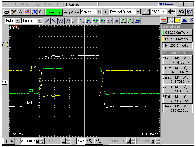
Figure 10. Measurement of the DATA1/NDATA1 signal from the generator.
In Figure 10, C1 and C2 are two complementary PECL signals with amplitudes of approximately 450mV. These are our DATA1 and NDATA1 signals fed directly from the external generator to the inputs of the CSA8000. We are using the 20GHz sampling heads of the CSA8000. Several observations can be made from this data:
- M1 is a mathematical calculation of the differential signals C1 - C2. The amplitude is 900mV, and the 10%/90% rise and fall times are close to 700ps. So this means that we have a clean set of DATA1/NDATA1 signals.
- We are also measuring the Crs or zero-crossing point of the differential signal M1. This is noted as 29.56ns. The scope is triggered, and all we want is one of these crossing points. We will power up the MAX9979 and measure the same crossing point, as it is delayed through the entire board.
- This delay also includes the delay of our two input cables. Because these cables will also be used to measure the signal's delay through the board, their delays cancel out. Nonetheless, it is still best to use the smallest length cables, but their delays are not important for the propagation delay measurement.
Step 5. Power up the MAX9979EVKIT.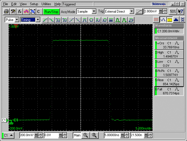
Figure 11. MAX9979 powered up and generating a 3V signal into the 50Ω load of the CSA8000.
Take the DATA1 and NDATA1 signals and connect them to the powered-up MAX9979EVKIT DATA1/NDATA1 inputs. Use the same cable as in Step 4. Set the MAX9979 to the specified 0V to 3V signal and terminate the output into 50Ω, as specified in the data sheet for the propagation delay measurement. In this case, the 50Ω load is the input to the CSA8000. Data points taken from Figure 11 then show:
- The output signal amplitude is now 0V to 1.5V. This is expected and is divided down by a factor of two by the 50Ω load.
- The rise and fall times are well within the specifications for the MAX9979. We are, therefore, assured that we have a good, clean, valid output driven by a very clean and valid DATA1/NDATA1.
- The setup for the CSA8000 remains as in Step 5. The trigger is the same, as in Step 4. Now we see that the zero-crossing point is 33.77ns.
Step 6. Calculate the MAX9979's propagation delay.
The total delay through the MAX9979EVKIT was:
33.77ns - 29.56ns = 4.21ns
To make this measurement:
- Subtract the DATA1 PCB run of 0.695ns, and our delay is now 3.515ns.
- Subtract our DUT1 PCB run of 0.18ns, and our delay is now 3.335ns.
- Subtract the delay of the 2in cable to the CSA8000. This delay was 402ps, so our delay is now 2.933ns.
The nominal delay in the MAX9979 specifications for this setup is 2.9ns. Here we have established that the delay for the MAX9979 soldered to the board of this EV kit is 2.933ns, which is very close to what was expected.
Summary
This analysis has demonstrated that using TDR measurements for propagation delay offers several advantages:
- Very accurate propagation delay measurements.
- No active probes (avoids the inaccuracies that they introduce) are needed.
- Simple techniques can be used for most propagation measurements.
- Impedance measurements ensure correct impedances for connectors and PCB runs.
- Excess capacitance and inductance in the signal path can be analyzed with the TDR signals, and then used as feedback to redesign the board if necessary.
- Simplified modeling and simulation tools ensure correct interpretations and confirm the measurement setups.
- Use of good practices in measuring critical specifications.
As signal speeds rise, the errors and mistakes in timing measurements can cause incorrect planning decisions, device selections, and system design. The use of good practices in high-speed measurements is always a good subject to revisit. This article emphasizes these good practices.