An external op amp (MAX4322) enables this switch-mode boost converter (MAX668) to deliver output currents as high as 4A with efficiencies better than 90%. The op amp enables the circuit to regulate with respect to ground (instead of the -5.2V supply-voltage input), thereby avoiding the effect of input variaTIons on the -3.6V output.
When converTIng a negaTIve-output power supply to one with higher (less negaTIve) output, one has to ensure that the output voltage is not affected by variations in input voltage. All such supplies include an internal reference voltage that enables regulation of the output voltage, and this reference is usually referred to the most negative rail (ground). Thus, the output voltage of such a converter depends on the accuracy of its negative input supply voltage.
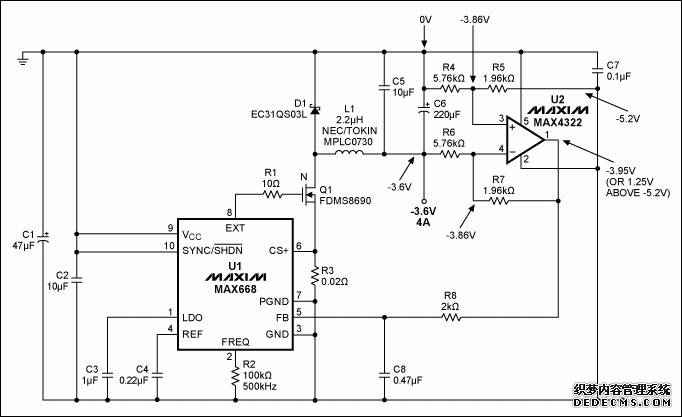
The circuit of Figure 1 does not have that limitation. Delivering output currents as high as 4A with efficiencies better than 90%, it generates a negative output with the help of an op amp and a switch-mode boost converter. Closed-loop feedback regulates the output voltage with respect to ground (the most positive rail), which is also the node from which current is delivered to the load.

Figure 1. This switch-mode converter generates a regulated negative supply voltage from a higher (more negative) input voltage.
The circuit converts a -5.2V supply voltage to -3.6V. The boost converter (U1) regulates its output voltage to maintain its FB voltage at -3.95V (1.25V above -5.2V). R8 and C8 form a lowpass filter that stabilizes the voltage at FB. You must then select the R4/R6 and R5/R7 pairs to produce the desired output voltage.
Making R4 equal to R6, and R5 equal to R7 improves the common-mode performance. The ratio of R4/R5 determines the voltage level at the positive input of the op amp (U2), whose closed-loop configuration ensures that the same voltage appears at its negative input. Knowing U2's output voltage (-3.95V) and its negative input voltage lets you determine the output voltage based on the values of R6 and R7: VOUT = -VREF(R6/R7), where VREF is the reference voltage of U1 (1.25V nominal), R4 = R6, and R5 = R7.
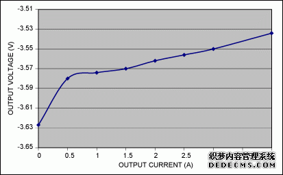
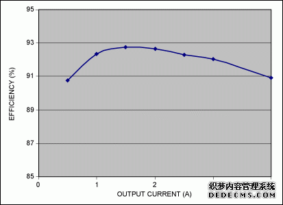
The component values shown, for example (R5 = R7 = 1.96kΩ, and R4 = R6 = 5.76kΩ), produce an output voltage of -3.76V. Performance is illustrated by graphs of output voltage vs. output current (Figure 2), and efficiency vs. output current (Figure 3).

Figure 2. Output voltage for the Figure 1 circuit varies with output current as shown.

Figure 3. Conversion efficiency for the Figure 1 circuit varies with output current as shown.