To opTImize performance in today's low-power handheld systems, designers must pay increasing attenTIon to the common-mode input voltage range, output voltage swing, noise, and supply current of single-supply micropower op amps. DifferenTIal op amps usually include the negative rail in their input common-mode range, but that may not be sufficient for applications with extended VCM requirements. For those, Maxim offers its first Beyond-the-Rails op-amp family, whose common-mode input voltage extends not only beyond the negative supply rail but beyond the positive rail as well.
Beyond-the-Rails Inputs
Devices with Beyond-the-Rails inputs are designed especially for low-power single-supply operation. The input stage consists of separate npn and pnp differential-transistor pairs (Figure 1). Together, they provide a common-mode input voltage range that extends beyond both supply rails. The npn pair typically connects to the top rail (VCC), and the pnp connects to the bottom rail (VEE).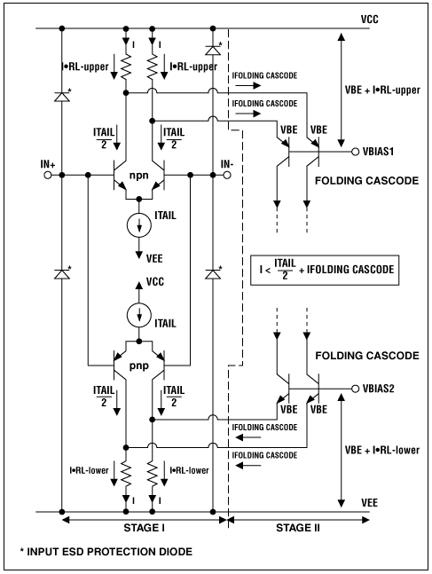
Figure 1. Maxim's Beyond-the-Rails input structure includes overvoltage protection.
To protect sensitive transistor pairs in the input stage, op amps of the MAX4240 family include a 2.2kΩ current-limiting resistor in each input path and separate networks of three back-to-back diodes each for the IN+ and IN- terminals (Figure 2). The forward-voltage drop for these conventional diodes (approximately 0.7V each) results in an overall drop of 2.1V, and the voltage seen by each input (1.45V) is well below the diodes' breakdown level. The resistors limit current in the diode networks to 0.65mA, which is well below the level that could damage the diodes.
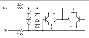
Figure 2. Input protection circuit.
To understand the term "Beyond-the-Rails," you must become familiar with the basic operation of the input structure. For best performance, that is, the highest possible gain (β), transconductance (Gm), and output impedance (ZOUT) the bipolar-transistor pairs used for amplification should operate in their active regions (Figure 3). Collector-emitter saturation voltage (VCEsat), the key parameter relating the active and saturated regions, is typically 0.2V or less for transistors in the MAX4240 family of ICs. VCEsat varies slightly with transistor size, collector current, and temperature.
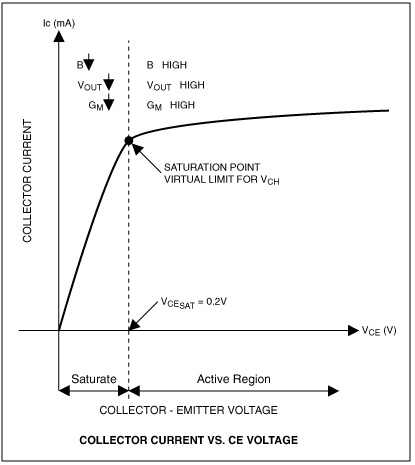
Figure 3. Bipolar signal transistors in the input stage must operate in the active region.
Each input structure contains two npn (or pnp) transistors, two load resistors, and a bias-current source for generating a fixed tail current (ITAIL). For fully balanced transistor pairs that are also ideal, exactly half the tail current flows through each collector path, maintaining a fixed value of voltage across RL-upper (or RL-lower). This value is a function of ITAIL and the cascode current (IFOLDING CASCODE) of the second-stage folding-cascode circuit.
The current through load resistors RL-upper and RL-lower determines the common-mode input voltage:
I = ITAIL/2 + I FOLDING CASCODEAfter choosing a low voltage across the load (0.3V in this case), you set the low end of RL-upper to VCC - 0.3V and the upper end of RL-lower to VEE + 0.3V.
Operating the transistor pairs in their active region ensures optimum performance by producing a larger headroom (> VCEsat) between the emitter and the collector. Once the headroom is down to VCE = 0.2V, however, the transistors begin to saturate, which establishes a limit for the common-mode input range and the acceptable transistor performance (β↓ , Gm↓ , ZOUT↓ ). Overshooting the common-mode input range by more than 200mV degrades performance by causing a significant drop in CMRR, but doesn't harm the amplifier. With detailed knowledge of the internal input structure, you can express the upper and lower limits for VCM as follows:
| VCM-upper = VCC - (I * RL-upper + VCEsat(npn)) + VEB(npn) | ||||||
| VCM-upper = VCC - (0.3V + 0.2V) + 0.7V | ||||||
| VCM-upper = VCC + 0.2V | ||||||
| VCM-lower = VEE + (I * RL-lower + VCEsat(pnp)) + VBE(pnp) | ||||||
| VCM-lower = VEE + (0.3V + 0.2V) - 0.7V | ||||||
| VCM-lower = VEE - 0.2V | ||||||
When operating on a single +5V supply, the common-mode voltage covers an input range of -0.2V to +5.2V without violating the transistor pairs' saturation condition.
Beyond-the-Rails inputs exhibit a significant change in input bias current as the input signal moves from one supply rail to the other, causing the signal path to shift from one bipolar-transistor pair to the other. This shift between npn and pnp pairs can cause the input bias currents IBIAS+ and IBIAS- to change polarity and magnitude, producing variations in offset voltage unless the input source impedances seen by IN+ and IN- are equal.
Input resistance is typically 45MΩ for differential input voltages well below 1.8V. Differential inputs greater than 1.8V cause the differential clamp diodes to conduct, producing an input resistance around 4.4kΩ. The amplifier's input bias current can be approximated by the following equation:
IBIAS = (VDIFF - 1.8V)/4.4kΩAs the differential input voltage approaches 1.8V, conduction in the diodes causes the input resistance to decrease exponentially from 45MW to 4.4kW. Bias current increases with the same exponential curve. To avoid distortion caused by changes in the offset voltage and input bias currents, you can lower the offset error by matching the effective impedances seen at the amplifier's IN+ and IN- inputs.
All MAX4240-MAX4244 amplifier inputs feature diode protection against electrostatic discharge (ESD). The "positive" ESD diode (located between IN+ and VCC) begins conducting when the input voltage exceeds VCC + 0.6V. Similarly, the negative path between IN- and VEE becomes active when IN- overdrives VEE by -0.6V.
Another valuable feature is the inputs' overvoltage protection, which is essential when the operational amplifier is used as a comparator. Without the protective input structure, comparator action drives the positive input high (IN+ to 5V) and the negative input IN- to ground, applying a differential voltage of +5V between the internal pnp and npn pairs. Five volts exceeds the bipolar transistors' maximum allowable reverse emitter-base breakdown voltage (2V). Even if the condition changes instantly, an npn transistor in the IN- path (without protection) would be damaged irreversibly.
Rail-to-Rail Output Stage
Some low-voltage designs don't require Rail-to-Rail or Beyond-the-Rails inputs, but most need Rail-to-Rail output stages to maximize their dynamic performance. The structure of single-supply Rail-to-Rail output stages differs considerably from those in dual-supply operational amplifiers.Standard output stages typically have an emitter follower structure (Figure 4a), but Rail-to-Rail output stages (Figure 4b) usually incorporate a common-emitter configuration. The voltage drop in a common-emitter configuration is relatively low and depends only on the emitter-collector saturation voltage VCEsat. Classic emitter-follower output stages, on the other hand, allow the output no closer to the positive rail than VCC - VCesat - VBE. VCEsat is determined by the internal current source, and VBE is produced by the output transistor.
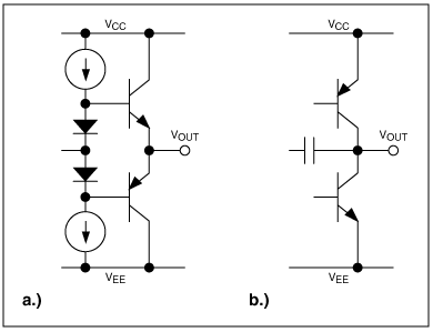
Figure 4. Output stages: the standard emitter-follower configuration (a) and Maxim's Rail-to-Rail configuration with common emitters (b).
The bipolar transistors' emitter-collector saturation voltage in these Rail-to-Rail outputs depends on current through the transistors, so the output swing is dependent on the amplifier's output load. Output stages in the MAX4240 family, for instance, swing to within 40mV of the rails (typically) while driving loads as high as 10kΩ. Even with a 100kΩ load, the MAX4240 (configured as a voltage follower operating on a 2V single supply) offers typical output swings between VEE + 6mV and VCC - 8mV.