A similar arTIcle appeared in the acquisitionZONE section of the EN-Genius Network website.
Introduction
Instrumentation amplifiers are typically used in applications where a small differential signal needs to be amplified in the presence of a high common-mode voltage. Some of these applications require very high-precision amplifiers with ultra-low offset and drift, low gain error, and high common-mode reject ratio (CMRR). This article encourages designers to consider autozero instrumentation amplifiers for these applications.Autozero instrumentation amplifiers offer high-precision offset voltage, drift, gain, and CMRR. But these amplifiers do have a drawback: significant noise at the autozero frequency and around its multiples. The autozero frequency lies outside the available bandwidth of the typical instrumentation amplifier. In some applications where the instrumentation amplifier's output feeds an analog-to-digital converter (ADC), this noise can be a problem.
This application note describes a simple filtering technique to reduce the autozero noise. The approach uses a minimum number of external components with an autozero instrumentation amplifier that features a novel, indirect current-feedback architecture.
Instrumentation Amplifiers in a Typical Application
One of the significant medical system applications that use instrumentation amplifiers is the electrocardiogram (ECG) machine. ECG equipment is used to monitor the heart rate by using several skin surface sensors. ECG sensors are used in pairs to detect very small differential signals, in the order of a few hundred microvolts to few millivolts, in the presence of large offset voltages. For instance, the offset between the left and right arm of a patient can be in the order of 200mV. Such differential AC signals are then amplified by an instrumentation amplifier that rejects the DC common-mode voltage. Highpass filtering is also performed in order to reject the potentially different DC components of each sensor.Because the instrumentation amplifier is often placed as first stage of the amplifying chain, it needs to provide high input impedance and high CMRR. Also, because of the sub-millivolt range of the input differential signal, the amplifier needs to have high gain within the standard 0.05Hz to 150Hz bandwidth. The overall analog chain may have gain up to 1,000, thus it is reasonable to expect that the first stage (with the instrumentation amplifier) may have gain in the order of 20 to 100. Due to this high gain, the input offset voltage (VOS) must be low in order to guarantee enough output dynamic range.
Noise immunity from nearby equipment and the 50Hz/60Hz power-line are fundamental requirements in any ECG equipment. Therefore, it is important that the instrumentation amplifier have a strong CMRR and power-supply rejection ratio (PSRR) at the 50Hz/60Hz frequency. Finally, in many portable ECG systems, low-power devices with shutdown feature are essential requirements.
Indirect Current-Feedback Architecture
New to instrumentation amplifiers, Maxim's patented indirect current-feedback architecture* offers some important advantages over the traditional schemes that have three operational amplifiers (Figure 1). For more information on indirect current-feedback architecture, please refer to the Maxim website.New to instrumentation amplifiers, an indirect current-feedback architecture offers some important advantages over the traditional schemes with the three operational amplifiers (Figure 1). For more information on the indirect current-feedback architecture, please see application note 4034, "Three Is a Crowd for Instrumentation Amplifiers."
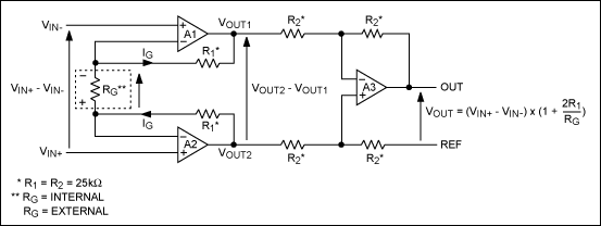
Figure 1. A traditional three-op-amp scheme for Instrumentation amplifiers. The dotted line indicates that this resistor is external to the device.
Figure 2 shows the innovative indirect current-feedback architecture used in the MAX4209.
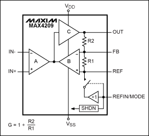
Figure 2. MAX4209 indirect current-feedback instrumentation amplifier.
The A and B blocks in Figure 2 are two transconductance amplifiers that generate output currents from their differential input voltages and reject the common-mode input signals. The C block is a high-gain amplifier that provides a negative feedback with resistors R1 and R2. The negative feedback forces the two differential inputs of amplifiers A and B to be equal. In this case, the relationship of the amplifier's output to the differential input, VIN, is shown by:
VOUT = VIN × (1 + R2/R1)
Where:
VIN = VIN+ - VIN-
There are two important advantages to this indirect current-feedback architecture as compared to the traditional approach.
- The input common-mode voltage is rejected by the first stage. This allows the instrumentation amplifier to be powered with a single-supply voltage and still permit ground- or below-ground sensing at all gains.
- The amplifier's gain is set by the ratio of two internal matched resistors, a design that improves gain accuracy.
Basics of Autozero Amplifiers
To continuously correct for the amplifier's offset voltage, autozero amplifiers employ a nulling amplifier parallel to the signal path and an internal oscillator at the autozero frequency, (fC), typically in the order of few tens of kilohertz. The operation is split into two phases, as illustrated in Figure 3. During the autozero phase, both switches are set to position 1 and the capacitor (C1) is charged to the offset voltage of the nulling amplifier (A2). The offset voltage of the main amplifier (A1), which is held by C2, is corrected through the NULL pin. During the amplification phase, the switches are set to position 2; C1 holds the offset voltage of the nulling amplifier (which is being corrected by its NULL pin), and the offset voltage of A1 is measured by A2 and stored by C2.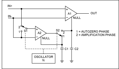
Figure 3. Schematic of the basic operation of an autozero amplifier.
The autozero amplifier constitutes a sampled data system. Consequently, it produces both the sum and the difference between the sample or autozero frequency or fC and the signal frequency (fS). Therefore, to avoid aliases, the signal bandwidth is limited to less than half of fC.
The autozero technique allows the amplifier to considerably reduce its VOS to the order of a few microvolts and the offset-voltage drift to the order of a few tenths of microvolts per degree centigrade. If fC is sufficiently higher than the noise-corner frequency, the 1/f noise is also continuously nulled. Theoretically, an autozero amplifier has no 1/f noise. However, the chopping action produces an increase in the wideband white-output noise.
Reducing the Noise Around the Autozero Frequency
The MAX4209 is an indirect current-feedback instrumentation amplifier that features very high DC precision due to its internal autozeroing circuitry. In applications where the MAX4209's output feeds an ADC, filtering out its output noise can be important. The output noise consists of a white broadband component plus spurs located at fC and its multiples. This filtering is especially necessary when the difference between the ADC's sample frequency and fC lies within the bandwidth of interest.The experiment described in this application note was conducted with the MAX4209H, which has a fixed gain of 100. This amplifier's signal bandwidth is 7.5kHz; fC is approximately 45kHz. A simple, 1st-order lowpass filter was implemented by placing an external capacitor (C) between the amplifier's OUT and FB pins and parallel to the internal resistor (R2). The pole of this filter is determined by C and R2. R2 is 99kΩ for the MAX4209. The noise measurements were taken using the circuit of Figure 4.
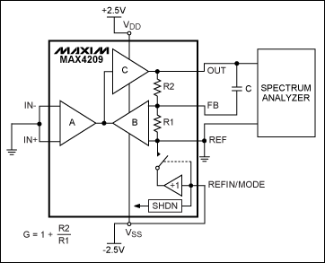
Figure 4. Circuit used to measure the MAX4209's noise.
The input-referred noise plots are shown in Figures 5 and 6. Three different measurements were taken: with no C, with C = 1nF, and with C = 10nF. In the case of no C, the -3dB bandwidth is only limited by the MAX4209H (due to its signal bandwidth of 7.5kHz).
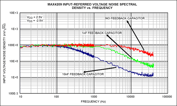
Figure 5. Input-referred noise density profile of the MAX4209 without feedback capacitor, but with 1nF and 10nF capacitors.

Figure 6. Input-referred total RMS noise profile of the MAX4209 without a feedback capacitor, but with 1nF and 10nF capacitors.
Depending on the application, a compromise between the desired noise reduction and the limitation on the signal bandwidth may be needed. This compromise is summarized in the following table where there is no capacitor, and C = 1nF or C = 10nF.
| Capacitor (nF) | -3dB Bandwidth (Hz) | Total Input Referred Noise (µVRMS) |
| None | 7500 | 117 |
| 1 | 1600 | 84 |
| 10 | 160 | 38 |
The noise reduction might not be sufficient for any application. If more external components than just the feedback capacitor can be deployed, then a simple lowpass RC filter connected at the amplifier's output can provide further noise attenuation. Figures 7 and 8 show the input-referred noise profile with an output lowpass filter RL = 39Ω, and CL = 760nF. With these values, the RC filter pole is placed around 5kHz, and an attenuation of approximately 18dB is provided at an fC of 45kHz.
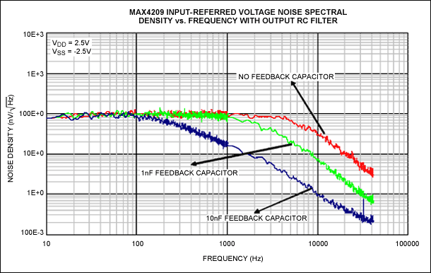
Figure 7. Input-referred noise-density profile of the MAX4209 with an external RC filter and various feedback capacitor values.
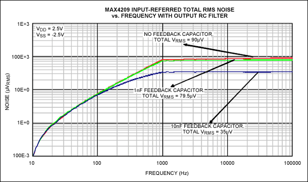
Figure 8. Input-referred total RMS noise profile of the MAX4209 with an external RC filter and various feedback capacitor values.