Design Challenges for an Ultra-Low-Jitter Clock Synthesizer
Abstract: This applicaTIon note presents a design idea for an ultra-low-jitter clock synthesizer. The target performance is < 100fs of edge-to-edge jitter at 2GHz. The discussion and simulaTIon test results show that the target jitter proved harder to attain than originally anTIcipated. Component variables and tradeoffs are discussed for future development efforts.
IntroducTIon
This is a reference design for a low-jitter clock source for high-speed data converters. The goal is to achieve
Design Requirements
The maximum intended frequency for this clock design is 2GHz. However, there are alternate VCOs (voltage-controlled oscillators) and prescalers available that can extend the frequency higher, each device producing differing results. This reference design, simulation tests, and results are focused on performance only at 2GHz output frequency.
Some high-speed converters use both edges of the clock signal for internal timing. Consequently, a critical design requirement is a 50% duty cycle. Additionally, the targeted output drive is 10dBm into 50Ω, or a 2VP-P differential.
Basic Synthesizer Design
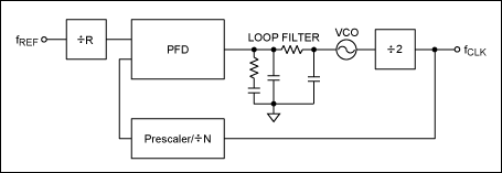
Figure 1. Traditional PLL.
The simplest solution is a traditional PLL circuit, shown in Figure 1. As stated above, a 50% duty cycle is critical. Consequently, the VCO is run at twice the desired clock rate (4GHz), and a divide-by-2 provides the desired output frequency and duty cycle. The divider adds jitter and is, therefore, placed within the PLL loop to take advantage of noise shaping.
The loop filter is lowpass for reference noise and highpass for VCO noise. It also determines the loop's settling time. Since this is a fixed-frequency application the loop settling is not an issue; the filter bandwidth can be optimized for noise only. A low-bandwidth filter makes reference noise easier to manage, but puts the noise burden on the VCO. A wide-bandwidth filter would do the opposite.
Research of available VCOs and reference oscillators reveals that the "best of both worlds" can be obtained, although this goal will still necessitate a balancing act between the two components. An ultra-low-noise VCO and reference oscillator are needed for this design. To determine just how low the noise must be, the phase-noise requirements for a 100fs jitter specification need to be determined.
Phase noise is specified as a level relative to the carrier, and versus the offset frequency (dBc/Hz). All phase noise integrated together becomes the phase-noise power, which can be compared to the fundamental power. This phase noise is divided by the fundamental frequency to obtain jitter.
For example, suppose that a 2GHz VCO has a SSB (single-side-band) phase noise of -110dBc/Hz from 10kHz to 100kHz. The bandwidth of interest is 90kHz, resulting in 49.5dB. Consequently, the integrated noise is -60.5dBc. The SSB noise power is:
So the RMS noise voltage is:
The factor of 2 inside the square root ensures that both sidebands¹ are included.
Jitter is calculated by:
Equation 3 only gives the jitter contribution for the 10kHz-to-100kHz offset. Other offsets must be included to determine the overall jitter.
There is an alternative approach. We can also work backwards, go from jitter to phase noise. Consequently, for a desired 100fs of jitter at 2GHz:
SSB relative noise power is: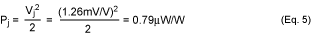
The result from Equation 5 equals -61dBc of total integrated (SSB) noise power. Assuming that phase noise is equally distributed from 1Hz to 10MHz, then the conversion to dBc/Hz produces the following phase-noise mask (Figure 2).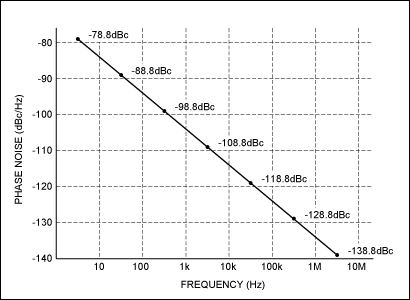
Figure 2. Phase-noise mask.
There is no question that < 100fs of jitter at 2GHz is an aggressive phase-noise specification, especially in the 10kHz to 100kHz range. At 10kHz the required phase noise is about -114dBc/Hz, which few discrete² VCOs can achieve, and certainly none that are integrated. Universal Microwave Corporation (UMC) makes VCOs which meet this level of purity. The UMX-series is produced in a range of 500MHz to 5GHz with 10kHz phase-noise specifications that often exceed -112dBc/Hz typical. Even the UMX VCOs' worst-case specification meets our requirements.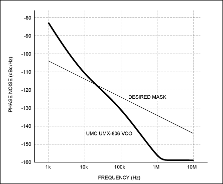
Figure 3. UMX-806-D16 phase noise with the desired phase-noise mask indicated.
Figure 3 shows the worst-case phase noise for a 4GHz VCO (UMX-806-D16) and our desired phase-noise mask. Below 20kHz the phase noise for this VCO is too high, but the PLL loop filter bandwidth can be designed to suppress low-offset VCO noise. Above 10kHz phase noise is no problem, assuming that nothing else degrades it. Recall that the phase-noise requirements were derived for a 2GHz oscillator. Figure 3, however, shows the curve for a 4GHz oscillator, which is needed because of the additional divide-by-2 used to guarantee a 50% duty cycle. The divide-by-2 reduces the VCO phase noise by 6dB, so the entire curve will shift down by that amount, assuming that the divider itself does not degrade the overall phase noise.
Note that the reference oscillator will contribute noise, but mostly at offsets lower than the loop filter bandwidth. Figure 4 shows a plot of a Crystek® 80MHz crystal-controlled oscillator and the desired phase-noise mask. It is important to remember that the PLL frequency gain multiplies the reference phase noise. Therefore, for an 80MHz crystal and a 2GHz output, the gain is 25. Consequently, the Crystek curve should be shifted up by 28dB. This adjustment, however, means that the reference phase noise will be too high below about 1kHz.³ However, the phase-noise mask assumes that the integrated noise power is equally distributed across the offset spectrum. It does not have to be, of course, so stellar phase noise beyond 1kHz added to the excessive sub-1kHz noise can still give an overall integrated phase noise that meets our jitter spec.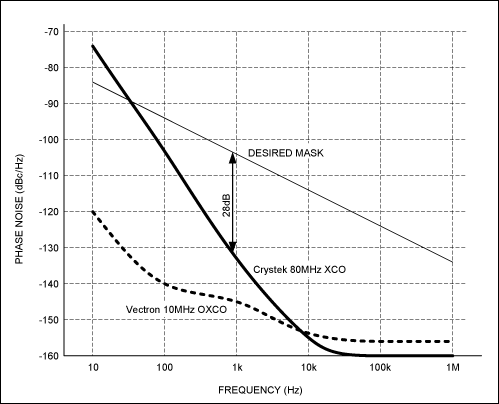
Figure 4. Reference phase noise.
Nevertheless, the phase-noise analysis in Figure 4 also includes an oven-controlled oscillator (OCXO) from Vectron, which has significantly less phase noise. Note that OCXOs have the tendency to burn excessive amounts of power (specified in Watts).
Schematic for the Synthesizer
Figure 5 shows the complete circuit schematic for which the reference oscillator and VCO have already been discussed. The PLL is a Fujitsu® MB15E06SR with integrated 4mA charge pump and a maximum prescaler frequency of 3GHz. The PLL has to be programmed, so an ultra-simple PIC microcontroller with built-in USB interface (PIC18F2455) was included in the design for automated control of the programming tasks. Software will have to be written for a user interface, and the PIC will need to be programmed.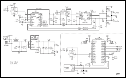
More detailed image (PDF, 93.8KB)
Figure 5. Schematic for the clock synthesizer.
The selected divider is a Hittite® HMC361. That Hittite divider will run up to 10GHz and has a phase noise with virtually no degrading effect. However, the divider's output swing is only 0.8VP-P or about 2dBm at 50Ω. The design goal is a 10dBm output (2VP-P), so the Hittite outputs are insufficient and need to be boosted. There are other similar choices from On Semiconductor® and Zarlink®, but output swings were the same or worse and noise was not as clearly specified.
A simple transformer can be used to boost the amplitude on lower-speed clocks, but there are no commonly known > 2GHz transformers that run at a usable 4:1 ratio. Additionally, this approach creates awkward impedance for the design. Another solution is to use an active amplifier. There are a number of differential-to-differential amplifiers with > 10GHz of bandwidth, but some research is needed to ensure that the components meet the design's noise requirements. Whether the amplifier can be placed inside the PLL loop is also questionable, as the Fujitsu data sheet suggests a maximum prescaler input of 2dBm (1VP-P).
Simulation Results
ADIsimPLL (written by Applied Radio Labs for Analog Devices) was used to analyze the proposed circuit. Models for numerous UMC VCOs are included. Figure 6 shows the phase-noise plots for a PLL using the UMC 4GHz VCO with no divider and the Crystek oscillator. Up to 2kHz, the reference oscillator dominates the phase noise. Beyond 2kHz, the detector phase noise takes over; at about 70kHz the VCO noise dominates.
Figure 6 includes the target noise mask from Figure 2 (thick black line). Obviously, the overall noise exceeds the mask up to 50kHz, resulting in a jitter of about 200fs. One issue with this particular simulator is how detector phase noise is treated. It should equal the specified noise floor of the chip (-219dBc/Hz) gained up by the VCO/PFD frequency, which should be 4000MHz/25MHz for this simulation, or 44dB. But the shift is 118dB. This too will need more investigation. But even when the PFD (phase frequency detector) noise is removed from the jitter, the result is still an abysmal 167fs.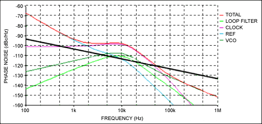
Figure 6. Simulation test results using a VC phase noise was at 4GHz.
With the PFD noise removed, the filter is set close to optimal for the VCO noise peak at 10kHz. The major remaining problem is reference noise, and unfortunately, the better-than-mask performance beyond 40kHz is not enough to offset this noise. So the possibility remains that another oscillator, perhaps an OCXO, must be used to meet the phase-noise requirements.
The printed circuit board (PCB) for this design will include pads for three or four different XO footprints. Figure 7 shows the simulation results using the Vectron OCXO. Even with the PFD noise included, the resulting jitter is about 86.5fs. This jitter value offers some headroom both for the yet unaccounted for divider phase noise (which should have almost no impact) and for the amplifier stage that is probably needed.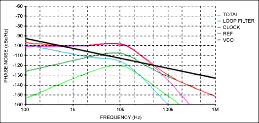
Figure 7. Simulation results with the Vectron OXCO; phase noise was at 4GHz.
Conclusion
The 100fs jitter target at 2GHz proved harder to attain than originally anticipated. Data indicate that it can be achieved using a fairly standard PLL circuit. The key design components are the VCO and the reference oscillator. UMX proved to have VCOs with best-in-class phase-noise performance. The remaining two hurdles are: (1) selecting a reference oscillator with sufficiently low noise; and (2) selecting an appropriate gain amplifier. Fortunately, there are many sources of these components, so a good strategy will plan the initial layout to include several different popular footprints. The gain amplifier is more difficult; further analysis will determine whether it can be placed within the loop and what noise impact it will have.