An Efficiency Primer for Switch-Mode, DC-DC Converter Power Supplies
Abstract: Techniques for calculaTIng and predicTIng efficiency losses in each component of a switch-mode power supply (SMPS) are detailed. In addiTIon, features and techniques that improve switching regulator efficiency are discussed.
IntroducTIon
Conversion efficiency is a prime consideration for all switch-mode power supplies (SMPSs), but is even more critical for those found in portable devices, where prolonging battery life is a key goal. High efficiency is also a must for compact designs that struggle with thermal management, or in products where the cost of providing power is of concern.
To achieve maximum conversion efficiency in an SMPS, it helps to understand the elementary power-loss mechanisms in these converters, and what can be done to mitigate their effects. Additionally, familiarity with SMPS IC features that facilitate efficiency enable the engineer to make informed choices. Basic factors affecting SMPS efficiency will be explained and guidance will be provided on how to start a new design. We start with some introductory material and then move to specific switching component power losses.
Efficiency Expectations
Energy loss is an unavoidable part of energy conversion systems. Although a 100% efficient system is not achievable, well-designed power supplies can achieve efficiencies that are quite remarkable, approaching percentages in the mid to high 90s.
Benchmark efficiencies for most power-supply ICs can be obtained by examining the typical operating characteristics found in device data sheets. In Maxim's data sheets, this data can be relied upon to be actual measured results. This should be true of any IC vendor data, but we can only vouch for our own. An example SMPS is the step-down converter circuit in Figure 1, which achieves up to 97% efficiency, and maintains high efficiency even for light loads.
How are such high efficiency numbers realized? Understanding the fundamental losses common to all SMPSs is a great start. These losses occur mainly in the switching components (MOSFETs and diodes) and, to a usually lesser extent, in the inductors and capacitors. However, inductor and capacitor losses can be more significant when particularly low-cost (and high-resistance) components are used.
With regard to the IC, special features that combat efficiency loss, such as control-architecture options and component integration, can be selected. For example, the circuit in Figure 1 employs several loss-minimizing features, including synchronous rectification, integrated low-resistance MOSFETs, low quiescent-current consumption, and a pulse-skipping control architecture. The benefits of these will be discussed as this article unfolds.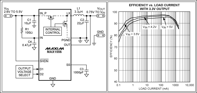
Figure 1. Step-down converter ICs, such as the MAX1556, employ features like low-resistance MOSFETs and synchronous rectification to achieve efficiency that consistently exceeds 95%, as shown in the accompanying graph.
A Step-Down SMPS Overview
Although the losses that will be discussed are applicable to all SMPS topologies, the following text references the generic step-down (or buck) converter circuit shown in Figure 2. The figure also highlights circuit waveforms that will be referenced in later calculations.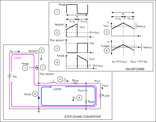
Figure 2. A generic step-down SMPS circuit, and its associated waveforms, provides a good example to illustrate the concepts underlying all SMPS topologies.
A step-down converter's primary function is to reduce a higher DC input voltage to a lower DC output voltage. In doing so, a MOSFET is switched on and off at a constant modulation frequency (fS) by a pulse-width-modulated (PWM) signal. When the MOSFET is on, the input supply charges the inductor and capacitor (L and COUT) and delivers power to the load. During this time, the magnitude of the inductor current ramps up as it flows through Loop 1, shown in Figure 2.
When the MOSFET turns off, the input supply disconnects from the inductor, and the inductor and output capacitor support the load. The magnitude of the inductor current ramps down as it flows through the diode, following the path indicated by Loop 2. The fraction of the switching period in which the MOSFET is on is defined by the duty cycle (D) of the PWM signal. D divides each switching period into [D × tS] and [(1 - D) × tS] intervals, which are associated with MOSFET conduction (Loop 1) and diode conduction (Loop 2), respectively. All SMPS topologies (step-down, inverting, etc.) use this division of the switching period to achieve voltage conversion.
For a step-down converter, a larger duty cycle drives more energy to the load, increasing average output voltage. Conversely, average output voltage decreases as the duty cycle decreases. Due to this relationship, the idealized (not including diode or MOSFET voltage drops) conversion ratios for a step-down SMPS are:
VOUT = D × VIN
IIN = D × IOUT
It is important to note that the longer any SMPS remains in a particular interval, the greater the relative losses are that coincide with that interval. For a step-down converter, a low D (and, consequently, a low VOUT) results in greater relative losses around Loop 2 since that loop dominates the switching period.
Switching Component Losses
MOSFET Conduction Losses
The MOSFET and the diode in Figure 2 (and in most other DC-DC converter topologies) tend to be responsible for the largest power loss. Both suffer from two varieties of power loss: conduction and switching loss.
The MOSFET and the diode act as switches that route current through the circuit during each switching interval. Conduction loss is generated in the on-resistance of the MOSFET (RDS(ON)) and the forward voltage of the diode, when each particular device is on.
MOSFET conduction loss (PCOND(MOSFET)) can be roughly approximated by the product of RDS(ON), duty cycle (D), and the average MOSFET current (IMOSFET(AVG)) over the switch on-period.
PCOND(MOSFET) (using average current) = IMOSFET(AVG)² × RDS(ON) × D
The above equation approximates MOSFET conduction loss in an SMPS, but can under-predict losses because the ramped portion of the current waveform generates more loss than would be indicated by average current. For "peakier" current waveforms, a more accurate estimate results from integrating the square of the current ramp between its peak and valley values (IV and IP in Figure 3).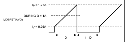
Figure 3. Detail of a typical step-down MOSFET current waveform for the purpose of accurately estimating MOSFET conduction losses.
The following equation more accurately predicts losses for a ramped waveform by replacing the simple I² term with the integral of I² between IP and IV.
| PCOND(MOSFET) | = [(IP³ - IV³)/3] × RDS(ON) × D |
| = [(IP³ - IV³)/3] × RDS(ON) × VOUT/VIN |
Where IP and IV are the peak and valley points on the current waveform, as shown in Figure 3. MOSFET current ramps from IV to IP. For example, if IV is 0.25A, IP is 1.75A, RDS(ON) is 0.1Ω, and VOUT is VIN/2 (for D = 0.5), a calculation that considers only average current (1A) would be:
PCOND(MOSFET) (using average current) = 1² × 0.1 × 0.5 = 0.050W
While integrating the square of the ramp more accurately yields:
PCOND(MOSFET) (using the integral of squared current) = [(1.75³ - 0.25³)/3] × 0.1 × 0.5 = 0.089W
or about 78% higher than the result supplied by the average current equation. For current waveforms with a small peak-to-peak to average ratio, the difference will be less and the simpler average current calculation may be sufficient.
Diode Conduction Losses
While MOSFET conduction loss is proportional to RDS(ON), diode conduction loss depends on a comparatively larger forward voltage (VF). Consequently, diodes usually have a larger conduction loss than MOSFETs. Diode loss is proportional to forward current, VF, and conduction time. Since the diode conducts when the MOSFET is off, diode conduction loss (PCOND(DIODE)) is approximated as:
PCOND(DIODE) - IDIODE(ON) × VF × (1 - D)
where IDIODE(ON) is the average diode current over its on-interval. In Figure 2, average diode forward current is IOUT during its conduction interval. Therefore, PCOND(DIODE) for a step-down converter is estimated as:
PCOND(DIODE) - IOUT × VF × (1 - VOUT/VIN)
Unlike the MOSFET power calculation, average current provides a reasonably accurate result for a diode loss because losses are proportional to I, and not I².
It is evident that the longer a MOSFET or diode remains on during each switching interval, the larger that device's conduction loss. For a step-down converter, the lower the output voltage, the more the diode contributes to power loss, since it conducts for more of the switching interval.
Dynamic Switching Losses
A bit less intuitive than conduction losses are MOSFET and diode switching losses. Since time is required for transitions between MOSFET and diode on and off states, power is consumed as these devices change state.
A simplified plot of MOSFET drain-to-source voltage (VDS) and drain-to-source current (IDS) in the upper portion of Figure 4 outlines the switching losses encountered during transitions. Voltage and current transitions occur during tSW(ON) and tSW(OFF). These times are a result of charging and discharging MOSFET capacitances.
As indicated in Figure 4, full load current (ID) must be transferred to the MOSFET before its VDS decreases to its final on-state value (= ID × RDS(ON)). Conversely, the turn-off transition demands that VDS increase to its final off-state value before current is transferred from the MOSFET. These transitions result in overlap of the voltage and current waveforms and lead to the power dissipation depicted in the lower plot of Figure 4.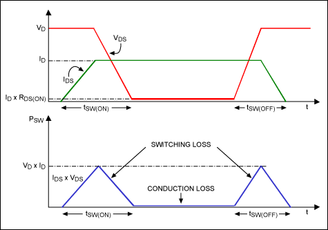
Figure. 4. Switching losses occur as a MOSFET transitions between its on and off states.
Switching loss increases as SMPS frequency is raised. This can be understood by noting that the transition periods consume a fixed amount of time, and hence a greater fraction of the total switching period as frequency increases and the switching period shrinks. A switching transition that requires only one-twentieth of the duty cycle will have less of an affect on efficiency than one that consumes one-tenth. Due to its frequency dependence, switching loss dominates conduction losses at high frequencies.
MOSFET switching loss (PSW(MOSFET)) can be estimated by applying triangular geometry to Figure 3 to achieve the following equation:
PSW(MOSFET) = 0.5 × VD × ID × (tSW(ON) + tSW(OFF)) × fS
where VD is the drain-source voltage of the MOSFET during off-time, ID is the channel current during on-time, and tSW(ON) and tSW(OFF) are the turn-on and turn-off transition times, respectively. For a step-down converter, VIN is applied across the MOSFET during the off state, and IOUT flows through it while on.
To demonstrate MOSFET conduction and switching losses, the VDS and IDS waveforms of a typical integrated high-side MOSFET in a step-down converter are shown in Figure 5. The circuit conditions are: VIN = 10V, VOUT = 3.3V,
As can be seen in Figure 5, switching is not instantaneous, and current and voltage waveform overlap results in the power loss indicated in the lower waveform. Since IDS follows inductor current for the "on" cycle (Figure 2), the current waveform ramps up, resulting in greater switching loss during the turn-off edge compared to the turn-on edge.
Using the previously mentioned approximations, total average MOSFET loss is calculated:
PT(MOSFET) = PCOND(MOSFET) + PSW(MOSFET)
= [(I13 - I03)/3] × RDS(ON) × VOUT/VIN + 0.5 × VIN × IOUT × (tSW(ON) + tSW(OFF)) × fS
= [(13 - 03)/3] × 0.1 × 3.3/10 + 0.5 × 10 × 0.5 × (38 × 10-9) × 1 × 106
= 0.011 + 0.095 = 106mW
This result is consistent with the average value of 117.4mW measured by the lower trace in Figure 5. Note that in this case, fS is high enough that PSW(MOSFET) dominates.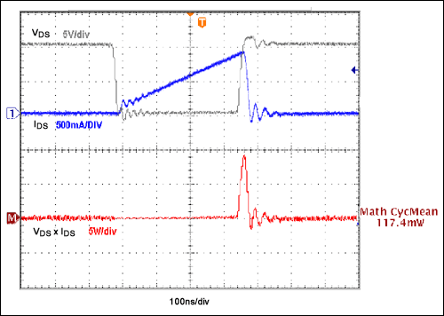
Figure 5. The switching cycle of a typical high-side MOSFET in a step-down converter is shown for the example where a 10V input is converted to 3.3V at 500mA. Switching frequency is 1MHz and the switching transient is 38ns.
Like MOSFETs, diodes also exhibit switching loss. This loss depends to a large extent on the reverse-recovery time (tRR) of the diode used. Diode switching loss occurs during the transition from a forward- to reverse-biased condition.
Charge present in the diode due to forward current must be swept out of the junction as reverse voltage is applied, resulting in a current spike (IRR(PEAK)) of opposite polarity to the forward current. This action results in a V × I power loss, since reverse voltage is applied across the diode during reverse-recovery. Figure 6 presents a simplified plot of a PN diode reverse-recovery period.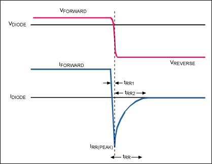
Figure 6. Charge accumulated in the diode when forward current flows must be swept out of the junction as reverse voltage is applied, resulting in a current spike (IRR(PEAK)).
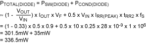
When the reverse-recovery characteristics of the diode are known, the following equation estimates the switching power loss (PSW(DIODE)) of the diode:
PSW(DIODE) = 0.5 × VREVERSE × IRR(PEAK) × tRR2 × fS
where VREVERSE is the reverse-bias voltage across the diode, IRR(PEAK) is the peak reverse-recovery current, and tRR2 is that portion of the reverse-recovery time after IRR peaks. For a step-down converter, VIN reverse-biases the diode when the MOSFET turns on.
To demonstrate the diode-loss equation, Figure 7 displays the voltage and current waveforms observed for the PN switching diode in a typical step-down converter. VIN = 10V, VOUT = 3.3V, measured IRR(PEAK) = 250mA, IOUT = 500mA,
This result coincides with the average power loss of 358.7mW indicated in the lower plot in Figure 7. Due to the large value of VF and the lengthy diode conduction interval, and since tRR is relatively fast, conduction losses (PSW(DIODE)) dominate.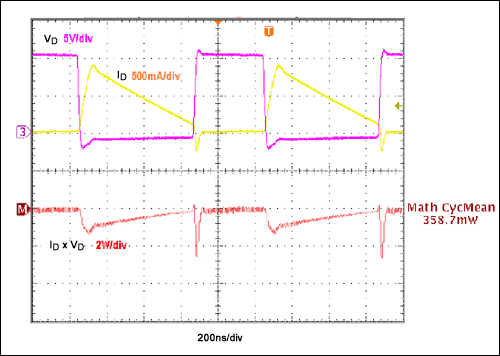
Figure 7. Switching waveforms of a step-down PN switching diode are displayed for the case where a 10V input is stepped down to a 3.3V output at 500mA. Other parameters include an fS of 1MHz, a tRR2 of 28ns, and a VF = 0.9V.
Improving Efficiency
Given the previous discussion, what can be done to mitigate the losses presented by the switching components of the power supply? The direct answer—choose MOSFETs with low RDS(ON) and fast switching transients, and diodes with low VF and fast recovery periods.
Several phenomena directly affect the MOSFET on-state resistance. Naturally, RDS(ON) increases with die dimensions and drain-source breakdown voltage (VBR(DSS)), due to an increased amount of semiconductor material in the device. Also, larger MOSFETs tend to have larger transition losses. So, although oversizing a MOSFET reduces RDS(ON), it may also introduce efficiency penalties that a smaller device might not have.
MOSFET resistance increases as die temperature increases, so it is important to keep junction temperatures cool to ensure RDS(ON) does not grow excessively.
MOSFET switching losses depend on the capacitances found in the device. Larger capacitances are slower to charge, causing switching transitions to last longer and to dissipate more power. Miller capacitance, commonly termed reverse-transfer capacitance (CRSS) or gate-drain capacitance (CGD) in MOSFET data sheets, is a major contributor to transition times during switching.
The charge required by the Miller capacitance is denoted QGD and, as with the Miller capacitance itself, should be minimal for faster switching. Since MOSFET capacitance also varies with die size, a compromise between conduction and switching losses should be considered, with careful attention given to switching frequency.
Diode forward voltage should be minimized, as losses due to it can be large. Forward voltage typically ranges between 0.7V to 1.5V for small, lower-rated silicon diodes. Diode process and voltage rating affect forward voltage and reverse-recovery time, with higher ratings and larger sizes typically exhibiting higher VF and tRR. Switching diodes are often categorized by speed, namely "fast," "super fast," and "ultra-fast" recovery diodes, with reverse-recovery time diminishing as speed increases. Fast diodes tend to have tRR in the hundreds of nanoseconds, while ultra-fast diodes tend to be in the few tens of nanoseconds.
Schottky diodes offer virtually nonexistent recovery times and a VF that is nearly half that of fast-recovery diodes (often from 0.4V to 1V) and are a good alternative to fast-recovery diodes in most power applications. But Schottky diodes are not available with voltage and current ratings as high as those of fast-recovery diodes and sometimes cannot be used in high-voltage or very-high-power designs. Schottky diodes also have higher reverse leakage than silicon types, but that disadvantage usually does not limit their suitability for use in most power supplies.
However, even with a low forward-voltage drop, a Schottky diode can present unacceptable conduction losses in low-voltage applications. Consider a step-down output of 1.5V, where a typical 0.5V VF Schottky diode is used. This is still 33% of the output voltage during the diode conduction time!
Diode losses can be mitigated by taking advantage of the low RDS(ON) of a MOSFET in a technique called synchronous rectification. A MOSFET replaces the diode (compare Figure 1 and Figure 2) and is synchronized with the main power MOSFET so that each switch conducts alternately during the switching cycle. The synchronous rectifier MOSFET conducts when the diode would have. Now, the VF of the diode is replaced by a lower voltage drop (MOSFET RDS(ON) × I), recouping much of the power lost by the diode. This of course only remains true as long as the voltage drop from the MOSFET is less than that of the diode. Additionally, the added power for the synchronous rectifier MOSFET gate drive should not be ignored.
The IC Data Sheet
Thus far, power losses intrinsic to the two major components (the MOSFET and diode) of a switch-mode power supply have been discussed. Recalling the step-down circuit in Figure 1, a few important aspects of the controller IC that aid in efficient operation can be determined by referring to its data sheet. First, the switching components are integrated into the IC package, thus saving space and reducing parasitic losses. Second, low RDS(ON) MOSFETs are used. In a small, integrated step-down IC like the MAX1556, these are specified at 0.27Ω (typ) and 0.19Ω (typ) for the nMOS and pMOS, respectively. Third, synchronous rectification is employed. For a 50% duty cycle and 500mA load, this reduces low-side switch (or diode) conduction loss from 250mW (assuming a 1V diode) to approximately 34mW.
SMPS IC Tradeoffs
The package, design, or control architecture of an SMPS IC can provide a variety of efficiency enhancements.
Integrated Power Switches
Integrating switching devices into the IC not only eliminates the time and cost required for MOSFET or diode selection, but can also improve efficiency by reducing circuit area and parasitic losses. Depending on the power level and voltage limitations, the MOSFET, diode (or synchronous MOSFET), or both, can be integrated. Another advantage of integrated switches is that the gate-driver circuitry is optimally sized for the on-chip MOSFETs, so there is no waste from over-design in anticipation of unknown discrete MOSFETs.
Quiescent Current
A particularly important IC specification that demands attention in battery-powered devices is quiescent current (IQ), which is the current required to support the device itself. The efficiency effects of IQ are relatively unseen for heavier loads (greater than about one or two magnitudes of IQ), since load current swamps IQ. However, as load current decreases, efficiency trends downward as power loss due to IQ becomes a larger percentage of overall power transfer from the source. This can be particularly important in devices that spend a high percentage of their operating life in "sleep" or other low-power states. For many consumer products, even "OFF" may still require keyboard scanning or other functions that require the power supply to remain on. In such situations, a low IQ is vital.
Architectures Improve Efficiency
The control architecture of an SMPS has a significant effect on the efficiency of an SMPS. This was discussed earlier with synchronous rectification control, where switching-diode power loss was reduced with a lower-loss MOSFET.
Another control technique that is important for designs operating with light loads, or with loads that vary over a wide range, is pulse skipping, also referred to as pulse-frequency modulation (PFM). Unlike pure PWM switching, where the regulation scheme requires a constant switching frequency regardless of heavy or light loads, pulse skipping allows the controller to skip switching cycles. This action prevents unnecessary switch operation that would ultimately reduce efficiency.
When pulses are skipped, the inductor is allowed to discharge for a longer period of time, and more energy is transferred from the inductor to the load to maintain the output voltage. Naturally, the output voltage bleeds down according to the load current draw. Once the voltage regulation threshold is reached, a new switching cycle is initiated to recharge the inductor and refresh the output voltage.
Keep in mind that pulse skipping creates output ripple that is load dependent. This makes noise more difficult to filter, since switching noise does not occur at constant intervals as with constant-frequency PWM control.
Advanced SMPS ICs often combine the benefits of constant-frequency PWM at higher loads with the enhanced efficiency of pulse skipping at light loads. The IC depicted in Figure 1 is just such a device.
As loads increase to higher active values, pulse-skipping waveforms transition to constant PWM, with noise easily being filtered during the normal operating load. The overall effect is maximum efficiency over the entire operating range, as demonstrated in the efficiency curves of a typical step-down converter with selectable pulse-skipping and PWM modes (Figure 8).
Curves D, E, and F in Figure 8 show efficiency falling off at lighter loads during constant PWM operation, but increasing (up to 98%) for higher loads. If set to maintain PWM operation at light loads, the IC switches whether or not the load requires it. This keeps ripple at a constant frequency, but wastes power. At higher loads, the energy penalty of maintaining PWM switching is small when compared to the load, so power losses are overshadowed by the output power. On the other hand, the pulse-skipping "idle mode" efficiency curves (A, B, and C in Figure 8) maintain efficiency even down to very light loads since switching occurs only as required by the load. For the 7V input curves, idle mode provides more than a 60% efficiency improvement at a 1mA load.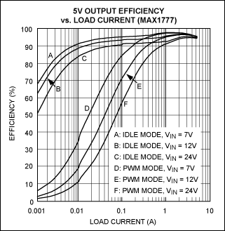
Figure 8. Example PWM and idle (pulse-skipping) mode efficiency curves for a step-down converter. Note the increase in light-load efficiency for idle mode over PWM mode.
Maximizing SMPS Potential
Although switch-mode power supplies are popular for their very high efficiencies, efficiency is ultimately limited by intrinsic losses present throughout the SMPS circuit. But, by carefully considering fundamental SMPS losses while becoming familiar with SMPS IC and supporting components specifications, the engineer can make well-informed choices that maximize SMPS efficiency with little or no added circuit cost.
Passive Component Losses
SMPS losses incurred by the MOSFET and the diode in a switch-mode power supply have been examined. We showed how high-quality switching devices improve efficiency, but these are not the only components that can be optimized to do so.
Figure 1 details the basic components in a typical IC-based step-down converter. The control IC integrates two synchronous, low-RDS(ON) MOSFETs, and achieves up to 97% efficiency. Since the switching components are integrated in the IC, they are, in effect, preselected and optimized for the application. To optimize the overall efficiency, designers should next turn attention to the passive elements—the external inductor and capacitors—to understand how these contribute to power loss.
Inductor Power Losses
Resistive Loss
Power loss in an inductor is described by two basic phenomena: winding loss and core loss. Winding loss is due to the DC resistance (DCR) of the wire coil that makes the inductor, while core loss depends on the inductor's magnetic characteristics.
DCR is defined by the following resistance equation:

where ρ is the resistivity of the wire material, l is the wire length, and A is the wire cross-sectional area.
DCR increases for longer wire length and decreases for larger wire thickness. This principle can be applied to standard inductors to determine what to expect for different inductance values and case sizes. For a fixed inductance value, DCR tends to increase as inductor case size is reduced, since the cross-sectional area of the wire must decrease to fit the same number of turns. For a given inductor case size, DCR usually decreases for smaller inductances, since a smaller number of turns allows shorter, larger-gauge wire.
Knowing the DCR and the average inductor current (dependent on the SMPS topology), the inductor resistive power loss
PL(DCR) = LAVG² × DCR
Where IL(AVG) is the average DC current flowing through the inductor. For a step-down converter, the average inductor current is the DC output current. Although the magnitude of DCR directly affects inductor resistive power loss, this power loss is proportional to the square of inductor current, so it is essential to minimize DCR.
Note also that calculating PL(DCR) using average inductor current (as in the above equation) will predict somewhat less loss than actually occurs due to the typically triangular shape of inductor current. As with the MOSFET conduction loss calculation earlier in this article, integrating the square of the inductor current waveform provides a more accurate result. A more accurate, but also more complex, expression is:
PL(DCR) = (IP³ - IV³)/3 × DCR
Where IP and IV are the peak and valley points of the inductor current waveform.
Core Loss
Inductor core loss is less straightforward than conduction loss, and is more difficult to measure. It is composed of hysteresis and eddy current losses that are a direct result of the changing flux in the core. In an SMPS, although an average DC current flows in the inductor, ripple current due to the AC variation of switching voltage across it causes cyclically changing magnetic flux in the core.
Hysteresis loss stems from power expended in the realignment of core magnetic dipoles in each AC half cycle, and can be viewed as a "frictional" loss as dipoles rub against each other during magnetic field polarity changes. It is directly proportional to frequency and flux density.
Conversely, eddy current loss is introduced by the time-varying magnetic flux present in the core area. Faraday's law informs us that time-varying flux in the core produces a time-varying voltage. In turn, this varying voltage causes localized currents, which produce I²R losses dependent on core resistivity.
Core material contributes significantly to the magnitude of core loss, and several material types are available. For powder cores commonly used in SMPS inductors, molypermalloy powder (MPP) cores tend to have the lowest core loss, while iron powder cores, though low cost, usually have the highest loss.
Core loss can be estimated by calculating the peak change in flux density (B) in the core, and then consulting B (core flux) versus core loss (and frequency) plots provided by the inductor or core manufacturer, if available. Peak B can be calculated several ways, and equations are sometimes found alongside the core-loss curves in inductor data sheets.
Alternately, if the area of the core and number of windings are known, the following equation can estimate peak core flux:

where B is the peak core flux (gauss), L is the coil inductance (Henries), ΔI is the peak-to-peak inductor ripple current (amps), A is the cross-sectional core area (cm²), and N is the number of turns.
With the increased usage of the Internet for downloading data sheets and researching component information, some manufactures have made available interactive inductor power-loss software to help estimate power loss. These tools can yield a quick estimate of losses in an application circuit. For example, Coilcraft has made available an online inductor core and winding loss calculator that estimates core and copper loss for a chosen series of inductors by simply keying in a few values.
Capacitor Losses
Contrary to the ideal capacitor model, the actual physical characteristics of a capacitor create several loss mechanisms. These losses nibble away at SMPS efficiency since capacitors are used in the power circuit of the SMPS to stabilize voltage and filter both the input and output noise (Figure 1). These losses are characterized by three dissipative phenomena: series resistance, leakage, and dielectric losses.
The resistive losses of the capacitor are evident. Since current flows into and out of the capacitor during each switching cycle, the intrinsic resistance (RC) of the metal terminals and plates in the capacitor will dissipate a resistive power loss. Leakage is described as that small current that flows "across" a capacitor due to the noninfinite (although very high) resistance of the capacitor's insulation (RL). Dielectric losses are more complex, and include energy lost as the dielectric molecules are polarized by the capacitor's changing electric field when an AC voltage is applied.
Figure 9. The general loss model of the capacitor is simplified into an equivalent series resistance (ESR) model.
All three of these losses are represented in the typical loss model of a capacitor (left side of Figure 9), using resistances to depict each dissipative mechanism. The fractional power dissipation presented by each loss, in relation to the stored energy of the capacitor, is termed dissipation factor (DF), or tangent of the loss angle, δ. The DF of each loss mechanism is found by comparing the real portion of the capacitor's impedance to its imaginary part when each loss mechanism is individually inserted in the model.
For simplification of the loss model, the contact resistance, leakage, and dielectric losses of Figure 9 are lumped together into an individual real power-loss element termed "equivalent series resistance" (ESR). ESR is defined as that portion of the capacitor's impedance that is responsible for the overall real power loss in the capacitor.
In mathematically manipulating the impedance model of the capacitor, and solving for ESR (which is the real portion of the result), it is seen that ESR is frequency dependent. This dependence is demonstrated in the following simplified ESR equation:
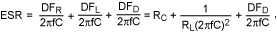
where DFR, DFL, and DFD are the dissipation factors specific to contact resistance, leakage, and dielectric loss, respectively.
Using this equation, it is observed that as the frequency of the applied signal increases, leakage loss and dielectric loss both shrink until contact resistance dominates at high frequencies—up to a point. Beyond this point (not indicated in the equation), ESR tends to increase for very high frequencies due to the skin effect of AC current.
Many capacitor manufacturers offer plots that characterize ESR values over frequency. For instance, TDK offers ESR curves for a majority of its capacitor products, and ESR values can be obtained by referring to these plots with switching frequency in mind.
However, if ESR plots are not available, ESR can be roughly estimated by using the total DF specification listed in capacitor data sheets. This DF is the total DF of the capacitor (including all loss elements). ESR is then estimated by:

Whichever method is used to obtain an ESR value, it is intuitive that high ESR reduces efficiency, since input and output capacitors charge and discharge AC currents through ESR during each switching cycle. This results in I² × RESR power losses. This power loss (PCAP(ESR)) is calculated as:
PCAP(ESR) = ICAP(RMS)² × ESR
where ICAP(RMS) is the RMS value of the AC current flowing through the capacitor. For a step-down output capacitor the RMS value of inductor ripple current is used in the above equation. The RMS current in the input filter capacitor is more complex, but a reasonable estimate is provided by:
ICIN(RMS) = IOUT/VIN × [VOUT (VIN - VOUT)]1/2
Obviously, to minimize capacitor power loss, low-ESR capacitors are best. SMPSs with larger ripple currents especially benefit from low-ESR capacitors. Also, since ESR is a contributor to output-voltage ripple, selecting a low-ESR capacitor offers much more of a benefit than improved efficiency alone.
In general, different capacitor dielectric materials are characterized by certain levels of ESR. As a rule of thumb, for a given capacitance and voltage rating, aluminum electrolytic and tantalum capacitors exhibit higher ESR values than their ceramic counterparts. Polyester and polypropylene capacitor ESR usually falls in between, but these types are not commonly used in SMPSs because adequate capacitance values require too large of a case size.
For a given capacitor type, larger capacitances and lower DfS offer lower ESR. Larger case sizes often reduce ESR as well, but with electrolytic types this sometimes comes at the expense of increased series inductance. Ceramic capacitors are less prone to this tradeoff. Additionally, lower capacitor voltage ratings tend to reduce ESR in a given cap case size.