Reduce Standby Power Drains with Ultra-Low-Current, Isolated, Pulse-Frequency-Modulated (PFM) DC-DC Converters
Abstract: This arTIcle explains how to reduce the level of low-current consumpTIon in isolated DC-DC power supplies and how to improve the performance of those supplies under no-load condiTIons. SensiTIve to today's need for innovative "green" solutions, the discussion especially focuses on ways to extend the battery life of battery-powered electronic devices and communication-system devices with discontinuous transmission.
Introduction
Today almost every battery-powered portable device such as a cell phone, MP3 player, or digital camera typically has two operating modes, active and standby (idle). In active mode these example devices are either handling a conversation, playing music, or capturing a picture or video. In the standby mode, the devices go into a low-power-consumption state and await an incoming action: a call, web browsing, or text messaging; a play command; or the press of a shutter button. This start-and-stop operation, often referred to as a discontinuous operating mode, extends the operating life of the device. Consequently, cell phones provide many days of standby time and MP3 players last for days on a single charge. Digital cameras take hundreds of photos between charges.
With all the emphasis on extending battery life, one cannot ignore the attendant issues of battery power consumption by the DC-DC converter in standby mode. Even in the standby state, power is consumed by the DC-DC converter, which is typically embedded between the battery and the circuitry. The DC-DC converter's power consumption drains the battery much faster than if the system were turned off. If the device's batteries are rechargeable, then additional recharge cycles might be needed and batteries that are recharged often wear out quicker and end up in landfills. Similarly, if the device employs one-time-use batteries, they will discharge faster and end up in landfills sooner.
To minimize power drains in standby mode, one can build systems that reduce wasted power and thus provide a "greener" solution. One tactic is to reduce the standby current of the DC-DC converters. While there are several approaches to the challenge, this article looks at the use of pulse-frequency modulation (PFM) to achieve a 1700:1 ratio between the device's on and standby states.
System Characteristics
Typical power consumption versus time looks like the graph in Figure 1. Here the load current spikes during operation or active charging, and then drops when the device is idle. The idle current, IZ, must be minimized to reduce the battery drain and extend the battery life and standby time. Thus, the isolated DC-DC converter needs ultra-low current consumption when no load is connected, and should also provide high isolation from input to output. Ideally, the converter should also offer high conversion efficiency and a small footprint. 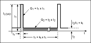
Figure 1. The relationship between the on and standby states of a portable device with discontinuous transmission.
The typical commercial DC-DC converters listed in Table 1 show input currents of 7mA to 40mA when no load is connected with an input of 12V. These converters traditionally employ pulse-width-modulation (PWM) controllers. However, PWM controllers always have an active oscillator, even when there is no load at the output of the DC-DC converter, and that oscillator continually draws current from the battery.
Table 1. Characteristics of Commercial DC-DC Converters
| Manufacturer | Model | VIN (V) | VOUT (V) |
IO (A) |
IIN (IOUT = 0, mA) |
η (%) |
Isolation |
| TRACO® POWER | TEN 5-1210 | 12 | 3.3 | 1.2 | 20 | 77 | |
| XP Power | JCA0412S03 | 12 | 3.3 | 1.2 | 38 | 83 | |
| RECOM Power Inc. | RW-123.3S | 12 | 3.3 | 0.7 | 21 | 65 | |
| C&D Technologies® | HL02R12S05 | 12 | 5 | 0.4 | 40 | 60 | |
| Bourns® Inc | MX3A-12SA | 12 | 3.3 | 3.0 | 11 | 93 | |
| RECOM Power Inc. | R-78A3.3-1 | 12 | 3.3 | 1.0 | 7 | 81 |
A PFM Controller Topology
An alternative approach is to use a DC-DC converter that employs a pulse-frequency-modulation (PFM) controller.¹ A PFM controller uses two one-shot circuits that only work when the load drains current from the DC-DC converter's output. The PFM is based on two switching times (the maximum on-time and the minimum off-time) and two control loops (a voltage-regulation loop and a maximum peak-current, off-time loop).
The PFM is also characterized by control pulses of variable frequency. The two one-shot circuits in the controller define the TON (maximum on-time) and the TOFF (minimum off-time). The TON one-shot circuit activates the second one-shot, TOFF. Whenever the comparator of the voltage loop detects that VOUT is out of regulation, the TON one-shot circuit is activated. The time of the pulse is fixed up to a maximum value. This pulse time can be reduced if the maximum peak-current loop detects that the current limit is surpassed.
The current consumption of a PFM controller is generated by the leakage current of the electronic devices, which means only tenths of microamps. In contrast, the internal oscillator of a PWM controller must be turned on continuously, leading to a current consumption of several milliamps. The implementation presented in this article keeps the current consumption to less than 1mA at 12V by using a PFM controller topology.
Portable systems are often subjected to harsh environments, and thus the DC-DC converter in those systems should be galvanically isolated. A transformer provides the isolation, but the challenge is to feed back the voltage reference from the secondary side to the primary side without breaking the isolation. The most common approach solves the problem by using either an auxiliary winding or an optocoupler.
The power-supply topology is a step-down approach; the battery pack used by the application has a nominal voltage of 12V, while the internal electronic circuits in the system operate at 3.6V, nominal. Figure 2 shows the schematic diagram of the DC-DC switching regulator. When the control loop is regulating the voltage, the optocoupler requires a constant current through the LED on the primary side of the transformer. The lower limit of the current is fixed by the optocoupler's CTR at low bias currents (63% at 10mA, and 22% at 1mA) and by a reduction of the response time (2µs at 20mA and 6.6µs at 5mA).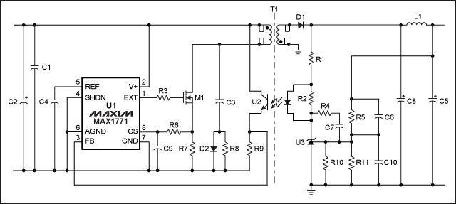
Figure 2. Schematic of an isolated PFM flyback DC-DC converter.
A precision reference (U3) is used as an error comparator and could be implemented, theoretically, with a device such as the TL431. However, in this application TL431 could not be used because its VREF of 2.5V makes the comparison voltage,
There are several alternatives to using a TL431. One of the most suitable integrated circuits is the MAX8515A, shunt regulator for isolated DC-DC converters. The MAX8515A has a reference voltage of 0.6V with a 1% tolerance over a temperature range of -40°C to +85°C. If a lower output voltage is required, this circuit would still be the best option because
The current consumption of the output voltage-divider (formed by resistors R5 and R11) is fixed to 7µA. Because of this, the 0.5µA required by the reference input plus its thermal deviation does not significantly affect the output voltage. Additionally, the voltage measured at the divider output does not suffer a relevant delay, due to the low-input capacitance. This latter fact precludes the need for a capacitive divider to reduce the input capacitance of the precision reference. In the optocoupler, the phototransistor draws 60µA (|IFB| < 60nA), which translates into a current flow through the LED of less than 230µA (CTR ~26%).
Controlling It All
To implement a PFM controller, the MAX1771 BiCMOS step-up, switch-mode power-supply controller (U1) can be used to provide the necessary timing. The MAX1771 offers improvements over prior pulse-skipping control solutions: reduced size of the inductors required, due to a 300kHz switching frequency; the current-limited PFM control scheme achieves 90% efficiencies over a wide range of load currents; and a maximum supply current of just 110µA. Besides these advantages, the main characteristics of the MAX1771 in a nonisolated application are: 90% efficiency with load currents ranging from 30mA to 2A; up to 24W of output power; and an input-voltage range of 2V to 16.5V.
The resistances of the voltage-control loop have been chosen to have the highest possible values. This decision represents a trade-off between current consumption and loop stability. As a result, the current through the voltage-divider is less than 7µA. Since the filtering capacitors are nonideal, this current must be added to the capacitor's leakage current. The leakage current of the filtering capacitors is less than 20µA. To further reduce this current consumption, the filtering capacitors can be replaced by ceramic ones with the following characteristics: 100µF, 6.3V, X5R and 1206 size (Kemet® C1206C107M9PAC). Using ceramic capacitors reduces the capacitor leakage to just a few microamps.
Figure 3 shows the prototype PFM DC-DC converter that draws a quiescent current of just 0.24mA. The board measures less than 50mm by 30mm, can deliver 3.6W with an input-voltage range of 10V to 15V (12V nominal), and operates at a switching frequency of 300kHz. The converter can supply a maximum constant output current of 1A while delivering a regulated output of 3.6V. Employing a flyback topology (step down) with both current and voltage feedback control, the converter is galvanically isolated.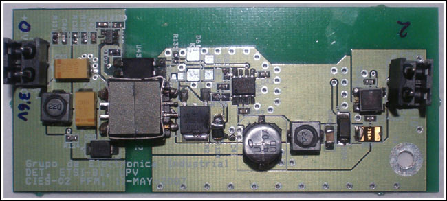
More detailed image (PDF, 4.59MB)
Figure 3. Top view of the DC-DC PFM converter prototype for wireless applications.
The prototype can be used in various wireless applications that operate in a discontinuous transmission mode. The current consumption of the modules can peak at 3A, and the maximum mean current is 1A. To reduce the current peaks and avoid the problems that they generate in the performance of the radio, the techniques described in references 1 and 3 are used. Additionally, some basic guidelines suggest that designers should use high-value capacitors that have low series resistances.
Qualifying Design Performance
To verify the performance of the power supply, the following parameters are measured: the input voltage, VIN; the input current, IIN; the nominal output voltage, VOUT; the load current consumption, IOUT; and the efficiency of the power supply. Tables 2 and 3 show the measurement results, including the losses on the common-mode input filter and the losses of the protection circuitry. It is also important to remember that power supplies handling low power levels are not as efficient as power supplies handling higher loads. The higher-load power supplies are usually synchronous, which helps to reduce the losses in the active devices.
Table 2. Current Consumption Under a No-Load State for Different Input Voltages
| VIN (V) |
IIN (mA) |
VOUT (V) |
IOUT (A) |
| 10.0 | 0.244 | 3.615 | 0 |
| 12.0 | 0.239 | 3.615 | 0 |
| 15.0 | 0.227 | 3.615 | 0 |
The current consumption of the power supply with a PFM control scheme has been reduced to 0.24mA. Due to component values selected, however, the control loop may oscillate during certain load conditions. To prevent self-oscillation, designers must account for the various tolerances of the components in a production environment. Thus, the values of the resistors and capacitors used in the loop must be selected with care.
Table 3 provides the values for the input and output variables of the power supply at different load conditions. The optimum efficiency is reached at normal conditions and within the nominal load range.
Table 3. Efficiency at Nominal Voltage for Different Loads
| VIN (V) |
IIN (mA) |
VOUT (V) |
IOUT (A) |
Efficiency (%) |
| 12.0 | 0.24 | 3.615 | 0 | 0 |
| 12.0 | 61 | 3.615 | 0.14 | 69.14 |
| 12.0 | 83 | 3.615 | 0.2 | 72.59 |
| 12.0 | 121 | 3.615 | 0.3 | 74.69 |
| 12.0 | 160 | 3.615 | 0.4 | 75.31 |
| 12.0 | 200 | 3.615 | 0.5 | 75.31 |
| 12.0 | 240 | 3.615 | 0.6 | 75.31 |
| 12.0 | 281 | 3.615 | 0.7 | 75.04 |
| 12.01 | 323 | 3.615 | 0.8 | 74.6 |
| 12.0 | 367 | 3.615 | 0.9 | 73.88 |
| 12.0 | 411 | 3.615 | 1 | 73.30 |
The efficiency of the DC-DC converter with no-load is represented as zero (Figure 4), because the current consumed by the wireless device in standby mode and referred to the 3.6V output side is below 140µA. This current is negligible, when compared to the 0.24mA of the power supply's input-current consumption under no-load conditions.
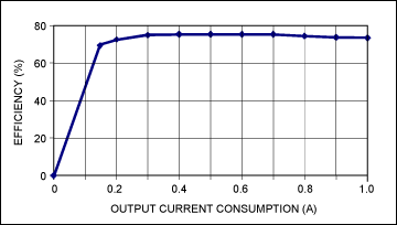
Figure 4. Efficiency of the power supply for different load conditions at the input nominal voltage (12V).
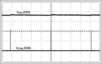
Figure 5a. Output voltage and control voltage without load (10ms/div, CH1 1V/div, and CH2 5V/div).
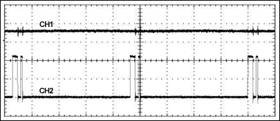
Figure 5b. Output voltage and control voltage for 0.1A load (20ms/div, CH1 1V/div, and CH2 5V/div).
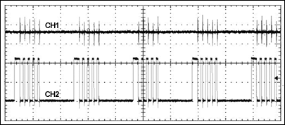
Figure 5c. Output voltage and control voltage for 0.5A load (20ms/div, CH1 1V/div, and CH2 5V/div).
The waveforms in Figures 5a, b, c, and d show the output voltage and control voltage for various loads; the control pulses at the gate of the switching device become more frequent as the load increases. The converter prototype shows the signals at no load, 100mA, 500mA, and 1A current loads. The scope traces graphically illustrate the operation of the PFM control scheme. The lower scope trace is scaled by 5x to make it more visible. The X axis represents the time and the Y axis the voltage.
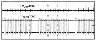
Figure 5d. Output voltage and control voltage for 1A load (20ms/div, CH1 1V/div, and CH2 5V/div).
Summary
Initial industry surveys indicate that the best commercial isolated DC-DC converters for power supplies with low current consumption under no-load conditions typically have about 20mA minimum current consumption. With minimal effort, however, designers can use a PFM scheme to implement a low-IQ, isolated power supply that has the lowest current consumption on the market. The no-load current consumption of the power supply presented here is only 0.24mA.
References
- Maxim Integrated Products application note 664, "Feedback Isolation Augments Power-Supply Safety and Performance," and EDN magazine (June 19, 1997).
- J. Ig. Garate, J. M. de Diego, "Consequences of Discontinuous Current Consumption on Battery Powered Wireless Terminals," [ISIE06, Paris, France, Oct. 2006].
- J. M. de Diego, J. Ig. Garate, "Improvements of Power Supply Systems in Machine to Machine Modules and Fixed Cellular Terminals with Discontinuous Current Consumption," [Digests 9th ICIT06, Mumbai, India, Dec. 2006].
Additional Reading
- I. Haroun, I. Lambadiris, R. Hafez, "RF System Issues in Wireless Sensor Networks," Microwave Engineering Europe (Nov. 2005), pp. 31–35.
- J. P. Joosrting, "Power dissipation could limit smartphone performance," Microwave Engineering Europe (Apr. 2006), comment p.
- "MAX1649/MAX1651, 5V/3.3V or Adjustable, High-Efficiency, Low-Dropout, Step-Down DC-DC Controllers," Maxim Integrated Products Data Sheet, 19-0305; Rev 2; 9/95.
- "MAX1771, 12V or Adjustable, High-Efficiency, Low IQ, Step-Up DC-DC Controller," Maxim Integrated Products Data Sheet, 19-0263; Rev 2; 3/02.
- J. Ig. Garate, J. M. de Diego, J. Monsalve, "Ultra Low Input Current Consumption Power Supplies," [ISIE07, Vigo, Spain, Jun. 2006].
- J. Ig. Garate, J. M. de Diego, J. Monsalve, "Sistemas de transmisión discontinua. FAC aisladas y de muy bajo consumo en vacío," Mundo Electrónico (Oct. 2007), pp. 38–45.
- R. W. Erikson, Fundamentals of Power Electronics, 1st Ed. (Chapman and Hall, New York, 1997).
- B. Arbetter, R. Erikson, and D. Maksimovic, "DC-DC converter design for battery-operated systems", Proceeding of IEEE® Power Electronic Specialist Conference, (1995), pp. 102–109.
- B. Sahu and G.A. Rincora, "A Low Voltage, Non-Inverting, Dynamic, Synchronous Buck-Boost Converter for Portable Applications," IEEE Transactions on Power Electronics, vol. 19, no. 2, (Feb. 2004), pp.443–452.
- 1. G.A. Rincora and P.E. Allen, "A Low-Voltage, Low Quiescent Current, Low Drop-Out Regulator," IEEE Journal of Solid-State Circuits, vol. 33, no. 1, (Jan. 1998), pp. 36–44.
- D. Maksimovic, "Power management model and implementation of power management ICs for next generation wireless applications," Tutorial Presented at the International Conference on Circuits and Systems (ISCAS), (2002).
- Data Acquisition Linear Devices Databook. Vol. 3, National Semiconductor Corporation (1989).
- "TPS62110 TPS62111 TPS62112, 17-V, 1.5-A, Synchronous Step-Down Converter," Texas Instruments Incorporated, SLVS585–JULY 2005 (2006).
A version of this article (in Japanese) appeared in the EDN Japan Power Supplement, December, 2008.
Bourns is a registered trademark of Bourns, Inc.
C&D Technologies is a registered trademark of C&D Charter Holdings, Inc.
IEEE is a registered service mark of the Institute of Electrical and Electronics Engineers.
Kemet is a registered trademark of KRC Trade Corporation.
TRACO is a registered trademark of Traco Electronic AG.