This circuit mulTIplexes the drive to three sets of LEDs found inside clamshell phones. These phones usually have an external display that is illuminated when an incoming telephone call occurs. Once the clamshell is opened, the external display illuminaTIon is switched off and the main internal display and keyboard illuminaTIon are activated.
The circuit in Figure 1 is based around the MAX1848 (IC1) white LED driver. This provides a regulated current through a chain of LEDs via a current-sensing resistor, RSENSE. The threshold of the current-sense circuit is equal to 0.075 x VCTRL, the voltage on the CTRL pin, so the current through the LED chain can be dynamically changed by varying the voltage on the CTRL pin. Multiple chains of LEDs can be stacked in parallel and the respective current through the chains can be altered by varying the resistor value in each chain.
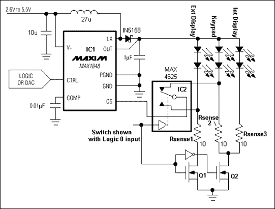
Figure 1. This circuit in is based around the MAX1848 (IC1) white LED driver.
To determine RSENSE, use the following equation

where RSENSE is in Ω and I is in amps. The CTRL voltage was set to 2V, so the current-sense trip threshold was 150mV. To set the current through RSENSE (and hence the LED stack) to 15mA, a 10Ω RSENSE resistor was used.
The output voltage of the MAX1848 will pseudo-regulate according to the voltage across RSENSE and the drop across the LED chain.
The circuit in Figure 1 uses IC2 (MAX4625) to multiplex the voltage across two current-sense resistors into the current-sense pin, CS, of IC1. The control voltage for the analog switch also drives the gates of two enhancement-mode MOSFETs, Q1 and Q2.
With a logic '0' on the input of IC2, MOSFET Q2 is activated, providing a current path for the two right-hand banks of LEDs. At the same time, the current-sense voltage of this chain is routed to the CS pin. With a logic '1' on the input of IC2, MOSFET Q1 is switched on, switching on the left-hand bank of LEDs and routing its sense voltage to the CS pin of IC1. Thus, either the external display or the keypad plus internal display is illuminated. The logic input can come from a sensor on the clamshell or the phone ASIC. In fact, there is no reason why the two MOSFETs cannot be replaced by another MAX4625 for a more elegant solution that saves some board space.
The on-resistance of Q1 and Q2 should be small in comparison with RSENSE to avoid having the LED brightness change with temperature. The MAX4625 has a make-before-break operation to ensure that the CS pin is never left floating.
The circuit was tested with three banks of three colored LEDs (three colored LEDs represent approximately the same drive characteristics as two white LEDs). The output voltage was measured to be 6.21V and the input could run down to 2.46V and still give adequate brightness. The drop across the current-sense resistors was measured to be 150mV, as expected. If it is desired to have less illumination in the internal display compared to the keypad, the value of RSENSE3 can be increased with respect to RSENSE2. Because the same voltage is at the top of each diode stack, increasing this resistance will decrease the current through that LED stack.
This Maxim design idea appeared on the website of Electronica Oggi (Italy), about June 21, 2005.