The Basics
No electronic component is perfect and the op amp is no exception. As usual, we assume an ideal op amp with the understanding that real-world limitations may need to be considered at some point.In particular, we assume infinite input impedance and zero output impedance. The front end of the circuit is not loaded in any way by the op amp and its output can source or sink as much current as needed to faithfully respond to the input. With these assumptions and op amp configurations with negative feedback, the voltage at the two inputs is identical and the output adjusts itself to a voltage to maintain this state.
It is also assumed that the bandwidth of the op amp is sufficient to respond to the needs of the circuit and the open loop gain of the amplifier is infinite.
The performance of modern components is such that in most cases, the above assumptions are perfectly acceptable and very little performance degradation occurs as we move away from the ideal.
Nodal Analysis
Long before the op amp was invented, Kirchoff's law stated that the current flowing into any node of an electrical circuit is equal to the current flowing out of it. (There are conditions on Kirchoff's law that are not relevant here.) An op amp circuit can be broken down into a series of nodes, each of which has a nodal equation. The equations can be combined to form the transfer function.Consider the circuit at the input of an op amp. The current flowing toward the input pin is equal to the current flowing away from the pin (since no current flows into the pin due to its infinite input impedance). The same cannot be said for the output, since the op amp can source or sink current.
Current-to-Voltage Converter
A simple current-to-voltage converter is shown in Figure 1. Its behavior can be easily understood using the previously explained nodal analysis. The input current (IIN) flowing into the inverting input is equal to the current flowing out of it through the feedback resistor (R). This current creates a potential drop across R, given as:V = IIN × R.
As explained earlier, the voltage at inverting input is equal to that applied at the noninverting input because the circuit has negative feedback; that is, the inverting input is fixed at VREF. This "virtual ground" at the inverting input implies that the op amp continuously adjusts its output voltage (VOUT) to maintain the IIN current flowing through R. VOUT is at VREF with zero input current, and it decreases proportionally for an increasing IIN. The following equation results:
VOUT = VREF - (IIN × R)
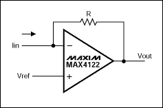
Figure 1.
Differential Amplifier
Taking this notion one stage further, Figure 2 shows a differential amplifier. Its transfer function can be calculated by again considering the currents flowing into and out of the nodes.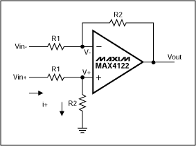
Figure 2.
Consider the current flowing towards the non inverting pin. This can be represented by:
Similarly, current flowing away from that node can be represented by
Combining Equation 1 into Equation 2 gives
Now, life is made easier if we use conductances instead of resistances (it keeps the fractions to a minimum). Thus,
where
so
therefore the voltage V+ is given by
The nodal equations for the inverting node are just as straight forward
To find a transfer function, we know
Combining Equation 3 and Equation 5 into Equation 4 gives
so
In other words, the output depends on the differential voltage across the inputs and the gain-setting resistors, as we would expect.
Wien Bridge Oscillator
The technique of nodal analysis can be used to analyze circuits with reactive components. In the same way we considered the conductances of resistors, with reactive components the equations are made easier by considering their admittances. A capacitor has an admittance of sC. Note that the Laplace nomenclature is used, since again it makes the equations look easier and the psychological effects of this are considerable. We could equally use jw in place of s if we wanted to get an idea of the phase effects of a circuit and this will be done later.Boldly going forth with the above supposition, a Wien bridge oscillator can now be analyzed. Figure 3 shows the generic configuration of this circuit. Again, to keep the equations simple most engineers keep the resistor values equal and the capacitor values equal. In this circuit we have both parallel and series networks, so it makes no difference to the simplicity of the math if admittances or reactances are used. The following analysis will keep with the preceding text and use admittances.
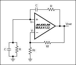
Figure 3.
Firstly, from Equation 3 the voltage at the inverting pin is
It is worth noting that if two admittances are placed in series, the total admittance is the inverse of the sum of their reciprocals (using the same formula as for two resistors in parallel). Similarly if two admittances are placed in parallel, the total admittance is sum of the admittances. Therefore the admittance from the output of the op amp to the non inverting input is
Likewise the admittance from the non inverting terminal to ground is
Using the methodology from before, it can be shown that (eventually)
Putting s = jw and R = 1/G gives
Therefore, using the principles of nodal analysis, the transfer function for the Wien bridge oscillator has been derived. From this equation two conclusions can be drawn, both of which are well known conditions for oscillation of the Wien bridge oscillator.
First, for oscillation to occur, there must be zero phase shift from the input to the output. This only happens at one frequency (when w = 1/CR). At this frequency the real terms of the numerator cancel and the phase shift represented by the imaginary terms in both numerator and denominator cancel (essentially, if you have no j terms in either numerator or denominator, there is no phase shift). Second, at this frequency the ratio of VOUT to V+ (hence V-) has to be 3. Anything less than 3 and the oscillation will decay. Anything greater than 3 and the output will saturate. This dictates the ratio of Gf to Gi to maintain oscillation: Rf must be equal to precisely twice the value of Ri.
Conclusion
Using Kirchoff's law, the currents flowing into and out of the nodes around the op amp can be translated into equations and from this the transfer function can be derived. The above examples use admittances instead of impedances, but the principles are the same and it is left to the engineer to decide which is more suitable. Once the equations have been derived, the math (depending on the complexity of the circuit) is moderately straightforward to obtain the transfer function. Then the power of math processing programs can be unleashed on the equations to find when, for example, instability occurs, or the susceptibility of the circuit to component variations, if this is desired.A similar version of this article appeared in the December 2002 issue of New Electronics magazine.