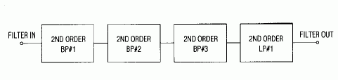
Figure 1. Cascaded, 2nd-order universal filter sections implement a C-message filter.
Dual universal, 2nd-order IC filters provide a compact and efficient means for implementing the circuit of Figure 1. If the IC filters are programmable, switched-capacitor types as shown, you can rapidly implement a C-message, psophometric, or other test filteres on demand simply by loading the chips with different sets of coefficients. These coefficients set each 2nd-order section's filter mode, Q, and cutoff or center frequency f0. The C-message filter has poles only, which are specified by the IEEE Standard 743-1984:
Table 1.
| Pole | Value in rad/sec | Value in Hz (f0) | Q |
| BP#1 | -1502 j1267 | 312.741 | 0.6540 |
| BP#2 | -2439 j5336 | 933.761 | 1.2027 |
| BP#3 | -4690 j15267 | 2541.886 | 1.7026 |
| LP#1 | -4017 j21575 | 3492.778 | 2.7316 |
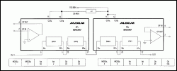
Figure 2 shows the external connections that configure two filter ICs in the architecture of Figure 1, along with a table of decimal equivalents for the digital coefficients assosiated with each filter section. These 2nd-order sections establish pole locations in accordance with the f0 values listed. Each section contains two continuous-time Chebysheff filters whose center frequency can be digitally programmed in 128 steps over the range 1 to 25kHz. Passband ripple is 0.1dB. For maximum signal-to-noise ratio, the signal amplitude at each section output should be as high as possible.
More Detailed Image
Figure 2. The circuit connections and coefficient sets shown enable two programmable, switched-capacitor filter ICs to realize the C-message filter of Figure 1. By loadingthe ICs with different coefficient sets, you can obtain the European psophometric noise-weighting filter and other test/measurement filters.
Signal swings are as follows: If you apply 4V to input INA on IC1, output BPA swings 2.7V, output BPB swings 1.85V, output BPA of IC2 swings 1.6V, and the lowpass output (LPA of IC2) swings 3.2V. IC2 operates in mode 4 instead of mode 1, which provides a gain of 2 instead of 1 for the LP and BP outputs (see data sheet)
You must bandlimit the filter's input signal to fCLK/4 or less, where (in this case) fCLK = 38.4kHz. The uncommited op amp in IC1 can provide second- or 3rd-order lowpass filter for this purpose. The uncommited op amp in IC2 can provide a similarlowpass filter for smoothing the output signal.
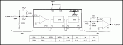
As an alternative, you can realize the C-message function using one filter IC and an external op amp (Figure 3). This approach lack flexibility, however. You can no longer switch to other filter functions by electrically reprogramming the circuit.
More Detailed Image
Figure 3. This circuit, based on one filter IC and an external op amp, produces the same C-message response of Figure 1 but lacks programming flexibility.
This circuit realizes the first bandpass (BP#1) in terms of external resistors and capacitors around uncommited opamp of IC1. BP#1, which also serves as an antialiasing filter for the samplin action of IC1, is an infinite-gain, multiple-feedback bandpass filter with f0 = 312.74Hz, Q = 0.654, and gain = 0.654. Design procedures for this configuration are available in the literature.
IC2 implements BP#2 and BP#3 with the same gain and signal levels as in Figure 1. The external op amp with resistors and capacitors implements LP#1, which also serves as the output smoothing filter. Like BP#1 you can design LP#1 as an infinite-gain, multiple-feedback circuit with f0 = 3492.778Hz, Q = 2.7316, and gain = 2.
The 125kHz clock frequency is arbitrary; other values require that you program IC1 for a different fCLK/f0 ratio.
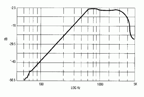
Figure 4. Circuits in Figure 1 and Figure 2 produce the same frequency response.
In both filter circuits (Figure 1 and Figure 2) the coefficients for f0A, f0B, QA, QB were calculated by software available from Maxim (see data sheet). Figure 4 shows the filter transfer function for either realization.