T7024蓝牙芯片的应用电路及封装管脚框图
T7024参考应用电路

T7024功能框图/T7024 Block Diagram

T7024蓝牙芯片管脚引脚定义:
Table 2-1. Pin Description
Pin Symbol Function
1 LNA_OUT Low-noise amplifier output
2 RX_ON RX active high
3 PU Power-up active high
4 R_SWITCH Resistor to GND sets the PIN diode current
5 SWITCH_OUT Switched current output for PIN diode
6 GND Ground
7 LNA_IN Low-noise amplifier input
8 GND Ground
9 VS_LNA Supply voltage input for low-noise amplifier
10 GND Ground
11 V3_PA_OUT Inductor to power supply and matching network for power amplifier output
12 V3_PA_OUT Inductor to power supply and matching network for power amplifier output
13 V3_PA_OUT Inductor to power supply and matching network for power amplifier output
14 GND Ground
15 RAMP Power ramping control input
16 V2_PA Inductor to power supply for power amplifier
17 V2_PA Inductor to power supply for power amplifier
18 GND Ground
19 V1_PA Supply voltage for power amplifier
20 PA_IN Power amplifier input
Slug GND Ground
T7024蓝牙芯片资料介绍
The T7024 is a monolithic SiGe transmit/receive front-end IC with power amplifier,
low-noise amplifier and T/R switch driver. It is especially designed for operation in
TDMA systems like Bluetooth and WDCT.
Due to the ramp-control feature and a very low quiescent current, an external switch
transistor for VS is not required.
相关热词:#电子电路图 #蓝牙芯片|T7024
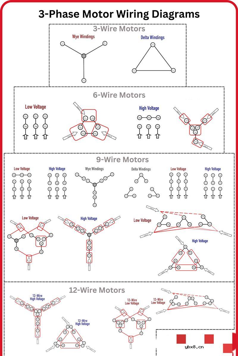 三相电机接线信息图
时间:2026-07-23
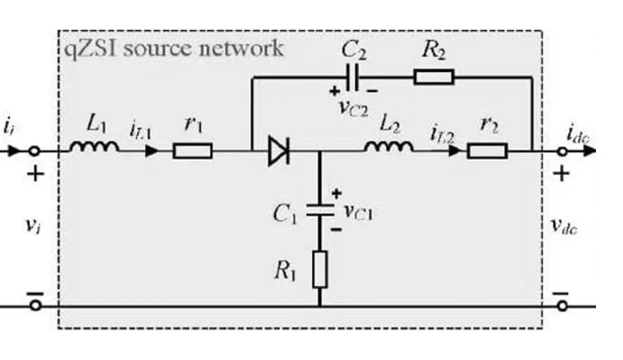 准 Z 源逆变器的设计
时间:2026-07-23
 关于阻容吸收器的简单介绍
时间:2026-07-23
S7-1200和CP343-1的Profinet通信方法
时间:2026-07-23
PDP(等离子显示),PDP是什么意思
时间:2026-07-23
光纤收发器的连接方式和作用
时间:2026-07-22
什么是电磁波?电磁波常见问题
时间:2026-07-22
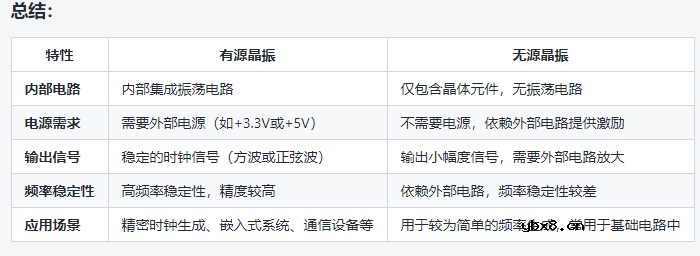 如何区分有源晶振和无源晶振
时间:2026-07-22
什么是“涡流”以及为什么它们对电机很重要...
时间:2026-07-22
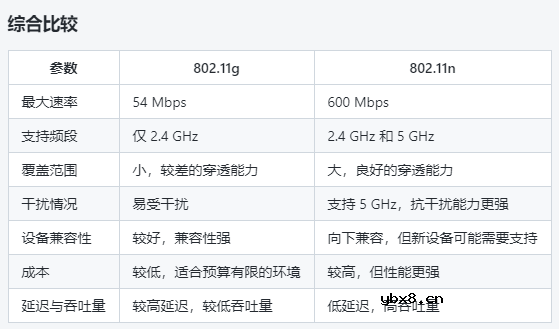 802.11g和802.11n的选择分析
时间:2026-07-21
电阻的单位
时间:2026-03-05
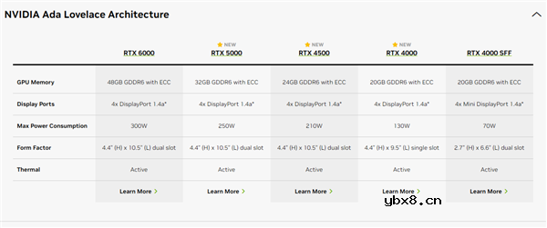 NVIDIA CPU+GPU超级芯片大升级!
时间:2026-03-09
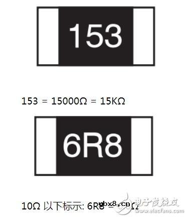 贴片电阻怎么看阻值
时间:2026-03-05
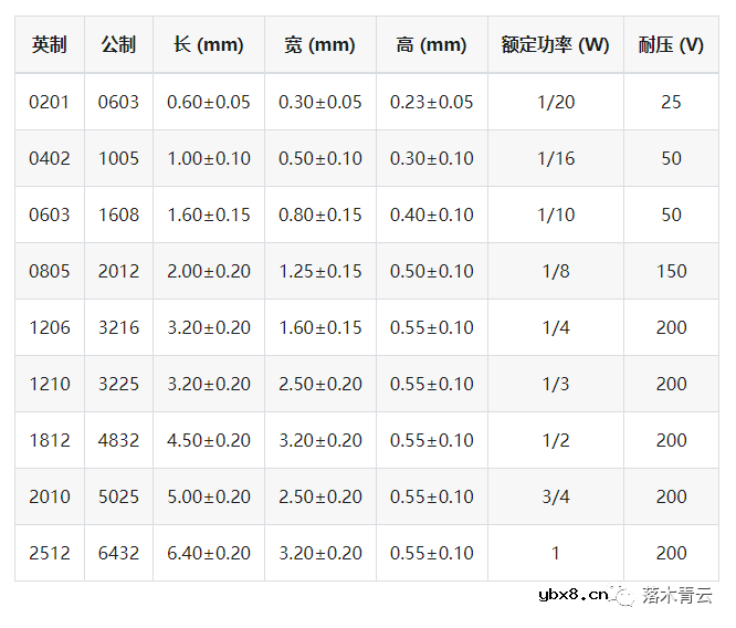 电阻的原理和作用 电阻色环识别图 电路中电...
时间:2026-03-09
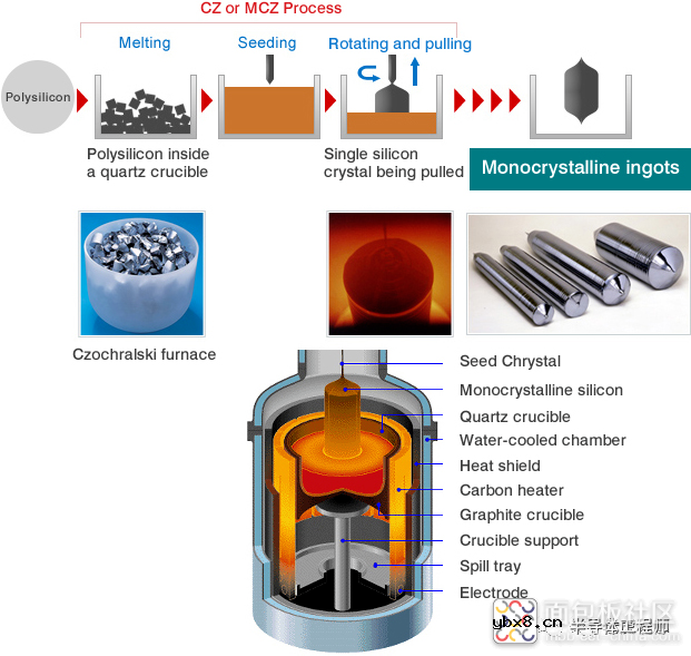 什么是硅片或者晶圆?一文了解半导体硅晶圆
时间:2026-03-09
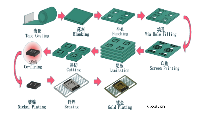 HTCC:半导体封装的理想方式
时间:2026-03-06
什么是室温超导?半导体时代将走向结束?芯...
时间:2026-03-09
 半导体光刻工艺 光刻—半导体电路的绘制
时间:2026-03-09
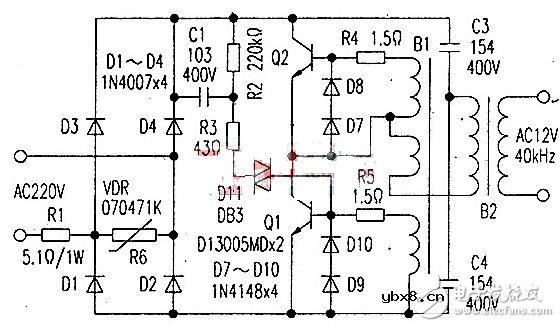 石英灯电子变压器电路原理
时间:2026-03-06
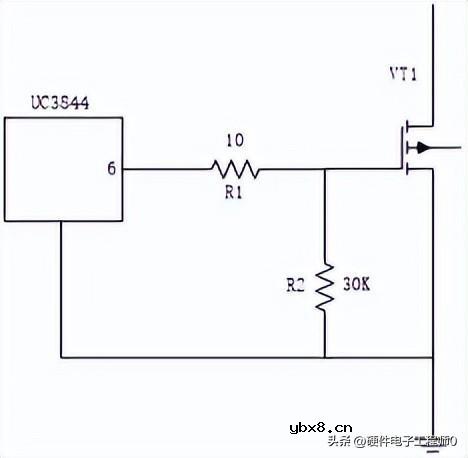 一文详解MOS管驱动电路拓扑的设计
时间:2026-03-09