
免费注册参加在线研讨会,学习如何分析、测量并最终解决音频系统的设计问题 (English only) 。
In its simplest form, a switch-mode amplifier consists of an H-bridge and a load (Figure 1). The H-bridge load includes the speaker impedance and a passive filter. The H-bridge steers current to the speaker, and the LC filter attenuates the switching noise. To understand more clearly why this method is better suited to portable devices than is the conventional linear amplifier, we must examine the advantages and pitfalls of each topology. Before making a full comparison, we first look at the characteristics common to all audio-specific output stages.
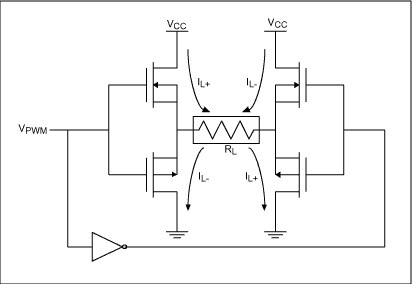
Figure 1. A Class D output stage uses MOSFET switches to alternate the current path to the load.
Amplifiers are typically classified by their output stages. Even with identical input and gain stages, amplifiers with different output stages exhibit different levels of performance and efficiency.
Of the common output-stage topologies (Classes A, B, AB, and D), Class D amplifiers exhibit the highest efficiency. A linear output stage (Class A, B, or AB) draws considerable bias current while sourcing and sinking current into a speaker. A nonlinear (Class D) output stage improves efficiency and extends battery life by eliminating this bias current, but efficiency is gained at the cost of greater noise and distortion. In portable equipment that allows linearity to be traded for efficiency, therefore, a Class D amplifier is the best choice.
Class A
The simplest and yet most effective approach (the Class A topology) consists of a bias transistor and a voltage-follower transistor. Because both transistors operate always in their active regions, such circuits produce lower distortion than does any other class of output stage, making them ideal for high-fidelity systems. Constant linearity is the Class-A topology's greatest asset and its Achilles heel as well. Efficiency suffers, because the high-side transistor draws appreciable current and the low-side transistor must be biased to handle peak currents at all times. At maximum signal levels, the maximum efficiency of a Class A stage is given by:This relationship assumes that the maximum output voltage is VCC, and that VCC = |VEE| (see Analysis and Design of Analog Integrated Circuits, by Grey and Meyer). Such an amplifier doubles as a space heater in high power applications and as a "gas guzzler" in battery-operated equipment.
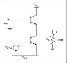
Figure 2. A Class A output stage exhibits the best linearity of all topologies, but draws the most supply current.
Class B
When compared with Class A, the Class B topology offers greatly improved efficiency at the cost of much higher distortion. Consisting of two transistors that are not active simultaneously, the Class B amplifier exhibits a maximum efficiency given by:Again, this equation assumes that the maximum output voltage is VCC and that VCC = |VEE|. Because this topology is not linear throughout its full dynamic range, it produces more distortion. Consider the circuit and graph in Figure 3, where the output stage consists of an NPN and a PNP transistor. As you sweep the input from VEE to VCC, the output passes through a dead zone of 1.4V in which both transistors are off. This dead zone causes crossover distortion. With a sine wave input applied to a Class B stage, the effect of crossover distortion is tantamount to the exclusion of every tenth word in this article.
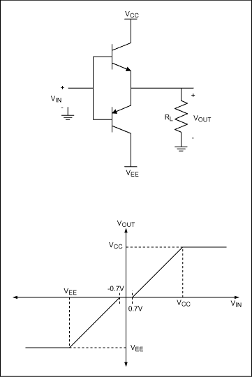
Figure 3. A Class B output stage is more efficient than a Class A, but exhibits crossover distortion.
Class AB
The output-stage topology most commonly used in monolithic audio amplifiers is Class AB. By adding bias circuitry to a Class B stage, the Class AB output stage drastically reduces crossover distortion while maintaining most of the Class B efficiency. Biasing improves linearity (which reduces distortion) by ensuring that at least one output transistor is active when the input is between E.7V and +0.7V. The efficiency (with respect to Class B) declines when both transistors are active simultaneously, but that is a small price to pay for markedly improved audio performance.Most of the other amplifier topologies available are not well defined. Indeed, similar designations for different schemes are in use by some manufacturers. Beyond Class A, Class B, Class AB, and Class D, the other types are either very esoteric or not applicable to audio amplifiers.
Class D
As mentioned earlier, linear amplifiers with similar input and gain stages can have dramatically different output stages. A Class D switch-mode amplifier, on the other hand, differs completely, input to output, from the linear amplifier. It resembles a switch-mode voltage regulator more than an amplifier.A Class D amplifier such as the stereo MAX4297 from Maxim consists of two input preamplifiers for filtering and level shifting, a sawtooth oscillator, two comparators, two MOSFET drivers, and two H-bridges (Figure 4). Each comparator samples the audio signal, with the oscillator frequency determining the duration of the sampling period. Thus, the oscillator frequency is an important factor in the overall performance of a Class D amplifier. The comparator output (Figure 5) is a pulse-width modulated square wave that drives the H-bridge. The H-bridge then outputs the square wave differentially, and provides a low-impedance source to the LC filter and load.
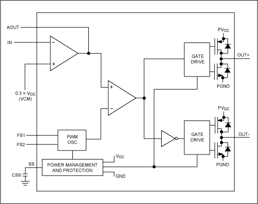
Figure 4. The MAX4295 monolithic Class D amplifier consists of an input amplifier, comparator, sawtooth oscillator, gate drivers, and internal power MOSFETs.
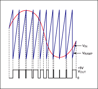
Figure 5. The PWM squarewave is created by a comparator whose inputs are the sawtooth (VRAMP) and the audio input (VIN).
Nonlinear Amplification, Signal Reconstruction, and THD
In contrast to conventional linear amplifiers, the Class D amplifier includes a comparator that breaks apart (samples) the audio input by comparing it against the sawtooth. During a switching period, the comparator output is low when the sawtooth exceeds the input signal and high otherwise (Figure 5). For clarity, the sawtooth frequency shown is relatively close to that of the audio, but usually it is much greater than the maximum audio frequency.For a given input level, the comparator output is a duty-cycle modulated square wave with period determined by the sawtooth frequency. It effectively samples the audio input. In addition to frequency, the amplifier's dynamic range is determined by the noise floor and the sawtooth magnitude. If the audio signal at the comparator exceeds the magnitude of the sawtooth, the resultant duty cycle is the same as if the signal were equal to the sawtooth. At the load, this condition appears as clipping.
The PWM signal controls the H-bridge drivers, turning opposite pairs of MOSFETs off and on, thereby reversing current to the load within a single period (Figure 1). As shown here, the signal in an audio amplifier is generally biased midway between the supply voltages. With no signal present, therefore, the comparator's output duty cycle is 50%. (This behavior is covered in the discussion on filters.)
It appears that the Class D amplification method distorts the signal. After all, THD is the result of nonlinearity in a circuit, and Class D stages break up the audio into nonlinear square waves. The output filter's averaging effect, however, enables Class D amplifiers to achieve THD figures <1%. The output filter is typically a 2nd-order LC lowpass filter, with cutoff frequency set just above the desired system audio bandwidth. It removes high-frequency content from the H-bridge squarewave output, and allows the amplified audio to pass through unchanged.
All lowpass filters have finite rejection in their stop-band, and a typical 2nd-order LC filter is no exception. A small amount of the switching frequency bleeds through to the load, but this is usually of no consequence because common audio transducers are incapable of reproducing such frequencies. Even if the speaker was capable of creating these high frequencies, the end user could not hear them. Other filter nonlinearities are within its own passband, and therefore produce a small amount of THD and noise. Prudent filter design can reduce these aberrations below audible levels.
Hear Only What You Want, and Filter Out the Rest
Proper filter design results in excellent amplifier bandwidth and THD performance. By attenuating the switching frequency and its harmonics, a filter with the right cutoff frequency and rolloff extracts the audio signal with minimal distortion. A filter with a 30kHz corner frequency, for example, passes 20kHz audio signals with less than 1dB of error, and 16kHz signals with less than 0.4dB of error. This loss of bandwidth is tolerable for most audio applications, because the typical adult cannot hear beyond 16kHz. The filter type should be chosen according to the demands of a given system, but the flat passband and good phase response of a Butterworth filter is a good choice for most applications.Output-filter design should be based on the frequency response desired for the system, and switching frequency is a major factor: lower frequency imposes a lower filter cutoff, and vice-versa. For example, a passive, balanced, 2-pole RLC filter with 30kHz cutoff frequency (Figure 6) is sufficient for a 250kHz switching frequency. Lower cutoff frequency reduces the amplifier bandwidth, of course, but that may be acceptable in a given application. Bandwidth loss may be intolerable in a radio or CD player, but high-frequency loss for voice amplification is not an issue if a 5kHz range is sufficient.
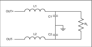
Figure 6. A balanced, 2-pole, lowpass Butterworth filter is ideal for most Class D applications.
Table 1.
The PWM square-wave output frequency from a Class D amplifier is beyond the response of the human ear and also of typical speakers, so the ear's bandwidth and the speaker's frequency response together serve as a sufficient filter for the switching frequency. If driving a speaker with high-frequency square waves produces decent audio quality, then, why does the Class D amplifier need an output filter? Because the elements of an external LC filter absorb the switching-frequency energy. Without a filter, this energy and the audio signal power must both be dissipated in the speaker.
Because a Class D amplifier continues to switch and provide current to the load even with no audio signal present, a speaker that is not robust can be damaged by the high frequency components of a Class D output. An output filter also reduces electromagnetic interference (EMI), which can become an issue if the output traces (or wires) are long and unshielded, or if EMI-sensitive components are located near the amplifier, or if amplifier and speaker are not in the same enclosure.
Oscillator Frequency
The frequency of the sawtooth oscillator is an important consideration in designing a Class D amplifier. The PWM output (switching) frequency determines both the output-filter requirements and the sampling rate for the audio input.The best balance between performance and component size is achieved with an oscillator frequency at least ten times the maximum signal frequency (which is typically 20kHz). A 250kHz switching frequency, for instance, allows moderately sized 15µH inductors and 1µF capacitors for a 4Ω load, to set the output-filter bandwidth at 30kHz. Such a filter attenuates the switching frequency sufficiently while allowing most of the audio signal to pass unattenuated to the load. For the MAX4295, a 250kHz oscillator frequency and 4Ω load yields a THD of 0.3% and an efficiency of 85%.
An oscillator frequency less than ten times the maximum audio signal can introduce distortion due to the amplifier's lower sampling rate: for a 20kHz audio input and 200kHz oscillator, the output signal is reconstructed with ten PWM periods per signal period. For a 100kHz oscillator, the output signal is reconstructed with five PWM periods per signal period. This difference may seem insignificant for a single-tone input, but the frequency of actual audio signals can vary widely in a short time, allowing a small portion of the input signal to be missed due to lower sampling and the output filter's averaging effect.
A lower oscillator frequency not only increases the reconstruction error, it requires a lower filter-cutoff frequency to sufficiently attenuate the switching frequency. Lower cutoff frequencies require larger component values, filling precious board space and increasing the overall cost. A lower cutoff frequency also reduces the amplifier's frequency range by increasing the attenuation of higher-frequency audio signals.
The greater distortion incurred by a lower oscillator frequency is offset by gains in efficiency. Switching losses are reduced because the MOSFETs do not switch as often, and that improves the efficiency (see Efficiency Losses). Conversely, a frequency far in excess of ten times the audio input reduces the filter size and improves distortion, but lowers efficiency. A higher oscillator frequency allows the filter cutoff to be higher, attenuating the switching noise sufficiently while allowing smaller component values. This condition lowers cost and component sizes for the output filter while extending the amplifier's frequency range.
Increasing the sampling rate reduces distortion to a certain extent, but slew rates for the comparator and bridge drivers become more important at high frequencies. A switching frequency of 1MHz has a period of 1µs, for example, assuming the comparator slews at 50V/µs and its output switches from 0 to +5V. With an output duty cycle of 50%, the average output voltage over the 1µs period, regardless of slew rate, is 2.5V. Reducing the duty cycle to 5% does not give the comparator's output enough time to reach 5V before the output state changes. The output rises to 2.5V in 0.05µs, then returns to 0V in the same amount of time. The averaged output is now 125mV, which is one half the expected 250mV. A similar behavior occurs when the duty cycle is 95%. Thus, the comparator's finite slew rate causes attenuation of the peak signal levels. Efficiency suffers at higher switching frequencies because the device switches more often (see Efficiency Losses).
100% Efficient, Theoretically
Class D amplifiers can be more design intensive than linear amplifiers, yet the benefit of efficiency justifies a more complicated system when simpler solutions already exist. The theoretical best efficiency for a traditional linear-amplifier output stage is 78% (as mentioned earlier), but linear amplifiers exhibit that efficiency only at their peak output power. The output stage of a Class D amplifier, on the other hand, delivers a maximum theoretical efficiency of 100% over its full dynamic range, and with sub-1% THD.Efficiency for a Class D output stage is attributed to the region of operation for its transistors. Output transistors in a linear amplifier operate in their active regions, but the corresponding transistors in a Class D stage require a certain level of bias current to buffer the voltage signal and drive current to the load. This bias current (not demanded by the load) lowers efficiency by causing extra power dissipation in the output transistors. Because voltage across the load is a function of the filter and the duty cycle of the PWM square wave (a 2-level voltage signal), the output transistors need only steer current to the load. This allows the output transistors, typically MOSFETs, to operate in their linear regions and draw zero bias currents.
IR losses (conduction losses) contribute the most power dissipation in a Class D output stage. Figure 7 shows the equivalent circuit for the stage during one operating state. RON is the MOSFET on-resistance, RP is parasitic resistance for the combined metal interconnects, bond wires, lead frame, and PCB traces, RF is the parasitic resistance of the filter components, and RL is the load. Given these values, the efficiency of the stage (ignoring switching losses) is:
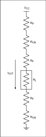
Figure 7. This DC equivalent loop shows the source of resistive losses in a Class D output stage.
Assuming no resistance in the components and traces except in the load, the efficiency of the Class D output stage is:
Because output power is directly related to IOUT and because the IOUT level is not a factor in the efficiency equation, the amplifier is theoretically 100% efficient over its entire dynamic range?a vast improvement over the conventional linear alternative.
The Real World
Unfortunately, ideal components do not exist and the Class D amplifier is not 100% efficient. Finite resistance in circuit elements is the most obvious contribution to power loss. A less obvious source of power dissipation is switching loss in the MOSFETs. As stated earlier, MOSFETs act like resistors when they operate in the linear region. Because they don't make instantaneous transitions from off to on, they spend a brief period during each cycle in the active region, where each draws extra current. The resulting power loss during one switching period (PSWITCH) is:where fOSC is the oscillator frequency, and tON and tOFF are the MOSFET rise and fall times. Switching at 1MHz consumes four times more power than at 250kHz. Considering resistive losses and switching losses, the efficiency for a Class D amplifier is therefore:
Based on this equation, you can roughly estimate the efficiency of a Class D amplifier as the ratio of RL to the other resistances in the circuit. Assuming RL = 4Ω, fOSC = 250kHz, tON = tOFF = 25ns, RON = 250mΩ, RF = 25mΩ, and RP= 80mΩ, η equals 86.33%. (Not 100%, but considerably higher than that of a conventional linear amplifier.) Increasing RL to 8Ω boosts the efficiency to a surprising 92.66%. These percentages do not account for power consumed by the front-end circuitry, the comparator, or the oscillator and drive circuits. That power loss has been ignored, because it is low with respect to power in the output stage.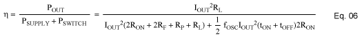
Measurements on a Class D amplifier such as the MAX4297, driving a 4Ω load over most of its dynamic range, shows efficiencies close to 85%. Efficiency decreases with output power because the quiescent current becomes larger with respect to the output current (Figure 8).
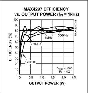
Figure 8. The MAX4297 efficiency improves as output power increases.
Conclusion
Most fully integrated switch-mode amplifiers are not intended for high-fidelity audio applications. Instead, devices such as the MAX4297 are intended for portable, battery-powered equipment such as cellular phones, portable radio/CD/tape players, MP3 players, laptop computers, PDAs, and portable DVD players. Consumers of those products are lured by the promise of portability and how long the device will last on three AA batteries, not by the expectation of a stunning, theater-quality audio experience. As the market for portable devices continues to grow and Class D amplifiers gain acceptance, you can therefore expect to see more switching amplifiers, featuring greater flexibility and higher levels of integration.A similar version of this article appeared in the August 2002 issue of Electronic Products magazine.